
VFM STEP-UP DC/DC CONVERTER WITH
VOLTAGE REGULATOR AND DETECTOR
1
RS5RJ SERIES
OUTLINE
The RS5RJ series are CMOS-based step-up DC/DC converter ICs equipped with a voltage regulator (VR) and
a voltage detector (VD). Each of these step-up DC/DC converter ICs consists of a VFM DC/DC converter, a linear
regulator and a voltage detector. These ICs are output-voltage-fixed type regulators which function as a linear
regulator when input voltage is high, and as step-up DC/DC converter + linear regulator when input voltage is
low, by using an inductor, a diode and a capacitor as external parts for the ICs.
Since a voltage detector is built in these ICs, the potentials such as the output voltage of DC/DC converters can
be monitored.
In addition, these step-up DC/DC converter ICs are suitable for battery-powered and hand-held instruments
because internal circuits can be turned off by the chip enable function so that the standby current can be mini-
mized.
∑
Low Supply Current...........................................Typ. 15µA (RS5RJ3624A : V
IN
=3.0V,at no load)
∑
Standby Mode .....................................................Istandby=Max. 1.0µA (RS5RJxxxxA)
Istandby=Max. 10.0µA (RS5RJxxxxB)
∑
Low Voltage Operation Possible .......................Operating Voltage V
IN
=1.2V to 10V
∑
High Output Voltage Accuracy .........................Fixed Output Voltage Accuracy±2.5%
∑
High Detector Threshold Accuracy...................±2.5%
∑
Output Voltage can be set at User's request (refer to Selection Guide).
∑
Voltage close to battery's voltage can be output because these ICs are of a step-up / step-down type
(Ex. a fixed voltage of 3V can be output by a 3V battery).
∑
Built-in Protection Circuits for Lx Driver
∑
Pin for External Driver is equipped, and a large current output can be obtained.
∑
Small Package ....................................................8pin SOP
FEATURES
APPLICATIONS
∑
Power source for cameras, camcorders, and hand-held audio equipment.
∑
Power source for small OA apparatus such as note type personal computers,and word processors.
∑
Power source for hand-held communication appliances such as pagers,cordless telephones, and cellular phones.
NO. EA-024-0204
2
SELECTION GUIDE
In the RS5RJ Series, the output voltage, the detector threshold, the version symbols, and the taping type for
the ICs can be selected at the user's request.
The selection can be made by designating the part number as shown below:
For example, the product with Output Voltage 5.0V, Detector Threshold 4.5V, Version A, and Taping Type T1,
is designated by Part Number RS5RJ5045A-T1.
RS5RJ
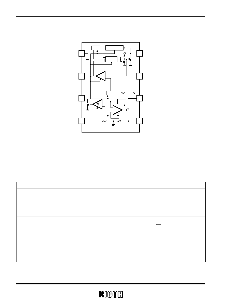
BLOCK DIAGRAM
≠
≠
≠
+
+
+
V
SS
CE
VD
OUT
VD
IN
Vref1
Vref2
VFM
OSC
1
2
3
4
5
6
7
8
L
X
EXT
V
DD
V
OUT
V
LX
Limiter
RS5RJxxxxx ≠ xx
Part Number
a b c
d
}
Code
Contents
Setting Output Voltage (V
OUT
):
a
Stepwise setting with a step of 0.6V in the range of 1.5V to 6.0V is possible.
b
Setting Detector Threshold Voltage (≠V
DET
):
Stepwise setting with a step of 0.1V in the range of 1.2V to 5.0V is possible.
Designation of Version Symbols:
c
A:
Operation of all the internal circuits is stopped by setting CE pin at V
DD
level.
B:
Operation of only Step-up DC/DC converter is stopped by setting CE pin atV
DD
level.
Designation of Taping Type:
d
Ex. 8pin SOP : T1, T2
(refer to Taping Specification)
"T2" is prescribed as a standard.
}
}

3
PIN CONFIGURATION
∑
8pin SOP
PIN DESCRIPTION
1
2
3
4
8
7
6
5
RS5RJ
Pin No.
Symbol
1
V
SS
2
CE
3
VD
OUT
4
VD
IN
5
V
OUT
6
V
DD
7
EXT
8
L
X
Pin Description
Ground Pin
Chip Enable Pin
Voltage Detector Output Pin.Nch Open Drain Output
Detection Input Pin of Voltage Detector
Output Pin for Regulator
Step-up Output. Power Supply Pin
External Transistor Drive Pin
External Inductor Drive Pin.

4
Topt=25∞C,Vss=0V
RS5RJ
ABSOLUTE MAXIMUM RATINGS
Symbol
Item
V
DD
Supply Voltage
V
LX
L
X
Pin Voltage
V
EXT
Output Voltage
EXT Pin Voltage
V
OUT
V
OUT
Pin Voltage
VD
OUT
VD
OUT
Pin Voltage
V
CE
Input Voltage
CE Pin Voltage
VD
IN
VD
IN
Pin Voltage
A Version
B Version
I
LX
Inductor Drive Output Current
Lx Pin Current
I
EXT
EXT Pin Current
P
D
Power Dissipation
Topt
Operating Temperature Range
Tstg
Storage Temperature Range
Tsolder
Lead Temperature (Soldering)
Rating
Unit
≠0.3 to +12
V
Vss≠0.3 to +12
V
Vss ≠0.3 to V
DD
+0.3
V
Vss ≠0.3 to V
DD
+0.3
V
Vss ≠0.3 to +12
V
Vss ≠0.3 to V
DD
+0.3
V
Vss ≠0.3 to V
DD
+0.3
V
Vss ≠0.3 to +12
250
mA
50
mA
300
mW
≠30 to +80
∞C
≠55 to +125
∞C
260∞C, 10s
Absolute Maximum ratings are threshold limit values that must not be exceeded even for an instant under any
conditions. Moreover, such values for any two items must not be reached simultaneously. Operation above
these absolute maximum ratings may cause degradation or permanent damage to the device. These are stress
ratings only and do not necessarily imply functional operation below these limits.
ABSOLUTE MAXIMUM RATINGS
5
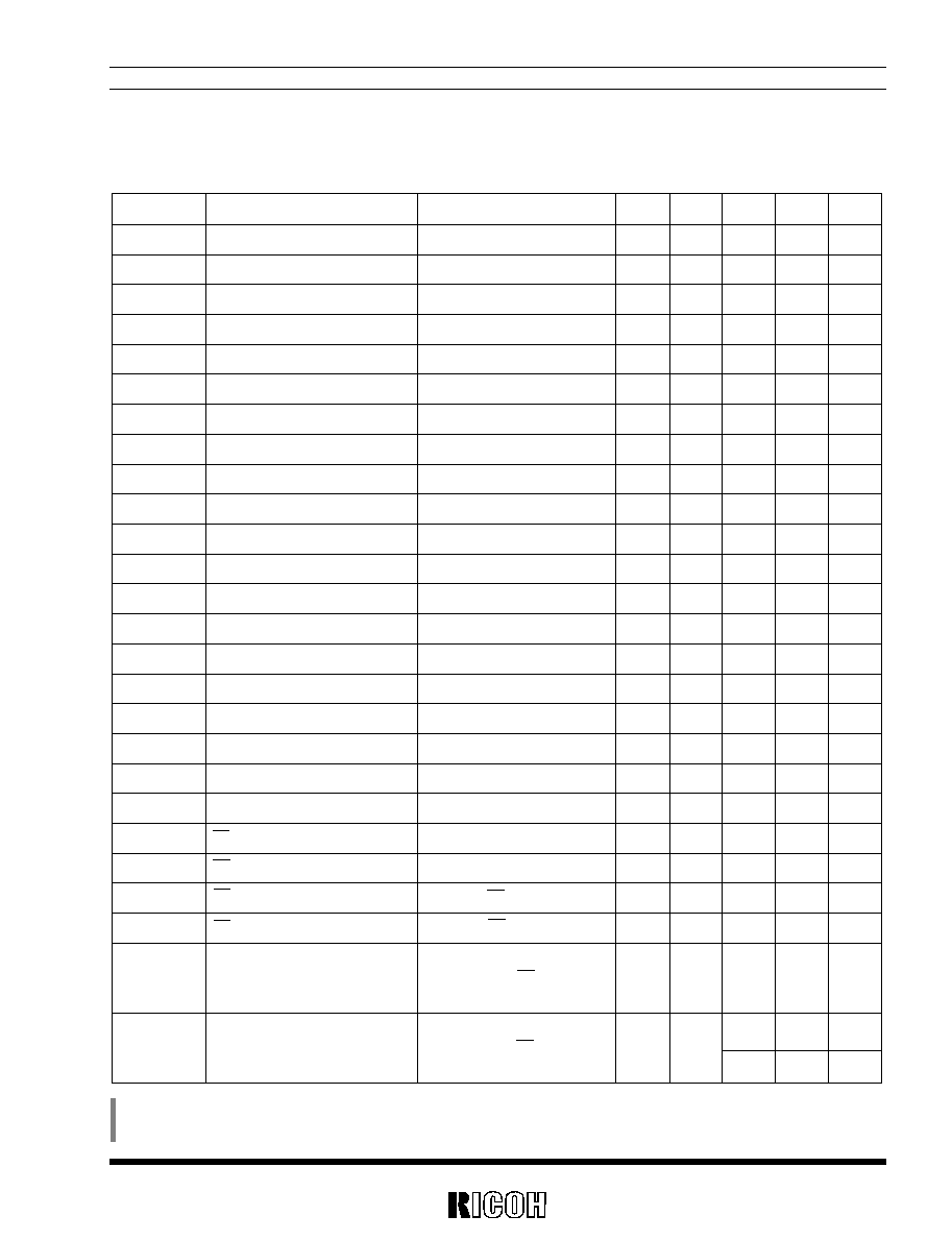
ELECTRICAL CHARACTERISTICS
RS5RJ
∑
RS5RJ3624A,B
Topt=25∞C
(Note 1) Standby current of Version A
(Note 2) Standby current of Version B
Please refer to Basic Circuit for Test Circuit.
Symbol
Item
V
IN
Operation Input Voltage
V
DD
Step-up Output Voltage
Voscst
Oscillator Start-up Voltage
Vhold
Hold-on Voltage
fosc
MaximumOscillator Frequency
Maxdty
Oscillator Duty Cycle
V
OL
1
Lx Output Voltage
I
OH
1
Lx Leakage Current
V
LX
lim
Lx Voltage Limit
V
OH
EXT Output Pch ON Voltage
V
OL
2
EXT Output Nch ON Voltage
V
OUT
Output Voltage
V
DIF
Dropout Voltage
V
OUT
/
I
OUT
Load Regulation
≠V
DET
Detector Threshold
V
HYS
Detector Threshold Hysteresis
V
OL
3
VD
OUT
ON Voltage
I
OH
2
VD
OUT
Leakage Current
I
VDINH
VD
IN
"H" Input Current
I
VDINL
VD
IN
"L" Input Current
V
CEH
CE "H" Input Voltage
V
CEL
CE "L" Input Voltage
I
CEH
CE "H" Input Current
I
CEL
CE "L" Input Current
I
DD
Supply Current
Istandby
Standby Current
Conditions
Min.
Typ.
Max.
Unit
Note
No load
1.2
10
V
No load
3.99
4.10
4.21
V
No load
0.9
1.2
V
I
OUT
=1mA
0.7
V
80
100
120
kHz
65
80
90
%
I
OL
=50mA
0.5
V
0.01
10.00
µA
L
X
Pin On
0.9
V
I
EXT
=≠3mA,V
DD
=4.1V
3.6
V
I
EXT
=5mA,V
DD
=4.1V
0.5
V
I
RL
= ≠5mA
3.51
3.60
3.69
V
I
RL
= ≠30mA
0.3
V
≠30mA
I
RL
0mA
100
mV
2.34
2.40
2.46
V
60
120
240
mV
I
OL
=5mA
0.5
V
0.01
5.00
µA
VD
IN
=V
DD
5
µA
VD
IN
=Vss
≠ 0.5
0.5
µA
V
DD
≠0.3
V
DD
V
0
0.2V
DD
V
CE=V
DD
≠ 0.5
0.5
µA
CE=Vss
≠ 0.5
0.5
µA
V
IN
=3V, L=100µH,
C=22µF, CE=Vss,
15
30
µA
No load
V
IN
=3V, L=100µH,
1.0
µA
Note1
C=22µF, CE=V
DD
,
No load
10.0
µA
Note2