 | –≠–ª–µ–∫—Ç—Ä–æ–Ω–Ω—ã–π –∫–æ–º–ø–æ–Ω–µ–Ω—Ç: RV5C386A | –°–∫–∞—á–∞—Ç—å:  PDF PDF  ZIP ZIP |

12345
12345
- 1 -
I
2
C-Bus Real-Time Clock ICs
with Voltage Monitoring Function
9.Jun.99
Preliminary
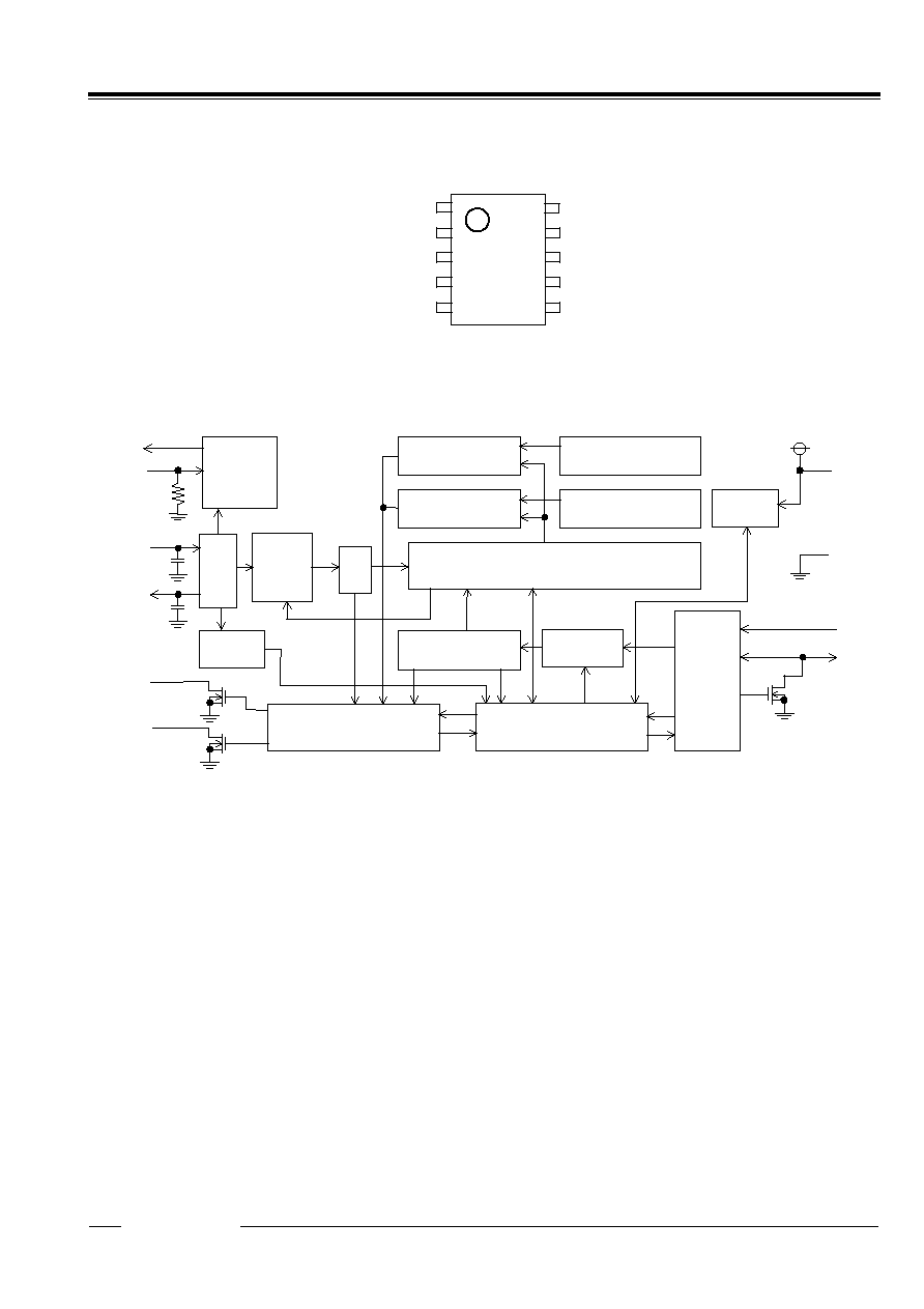
1. OUTLINE
The RV5C386A is a CMOS real-time clock IC connected to the CPU by two signal lines, SCL and SDA, and
configured to perform serial transmission of time and calendar data to the CPU. The periodic interrupt circuit
is configured to generate interrupt signals with six selectable interrupts ranging from 0.5 seconds to 1 month.
The 2 alarm interrupt circuits generate interrupt signals at preset times. As the oscillation circuit is driven
under constant voltage, fluctuation of the oscillator frequency due to supply voltage is small, and the time
keeping current is small (TYP. 0.35
µ
A at 3 volts). The oscillation halt sensing circuit can be used to judge
the validity of internal data in such events as power-on; The supply voltage monitoring circuit is configured to
record a drop in supply voltage below two selectable supply voltage monitoring threshold settings. The 32-
kHz clock output function (CMOS output) is intended to output sub-clock pulses for the external
microcomputer. The 32-kHz clock output can be disabled by certain input pin. The oscillation adjustment
circuit is intended to adjust time counts with high precision by correcting deviations in the oscillation frequency
of the crystal oscillator. This model comes in an ultra-compact SSOP10G (Pin Pitch 0.5mm, Height1.2mm,
4.0mm
◊
2.9mm).
2. FEATURES
∑
Timekeeping supply voltage ranging from 1.45 to 5.5V
∑
Low power consumption
0.35
µ
A TYP (0.8
µ
A MAX)
at VDD=3V
∑
Only two signal lines (SCL and SDA) required for connection to the CPU.
( I
2
C-Bus Interface, 400kHz at VDD
2.5V, address 7bits)
∑
Time counters (counting hours, minutes, and seconds) and calendar counters (counting years, months, days,
and weeks) (in BCD format)
∑
1900/2000 identification bit for Year 2000 compliance
∑
Interrupt circuit configured to generate interrupt signals (with interrupts ranging from 0.5 seconds to 1 month)
to the CPU and provided with an interrupt flag and an interrupt halt
∑
2 alarm interrupt circuits (Alarm_W for week, hour, and minute alarm settings and Alarm_D for hour and
minute alarm settings)
∑
32-kHz clock circuit (CMOS output, equipped with a control pin)
∑
Oscillation halt sensing circuit which can be used to judge the validity of internal data
∑
Supply voltage monitoring circuit with two supply voltage monitoring threshold settings
∑
Automatic identification of leap years up to the year 2099
∑
Selectable 12-hour and 24-hour mode settings
∑
Built-in oscillation stabilization capacitors (CG and CD)
∑
High precision oscillation adjustment circuit
∑
CMOS process
∑
Ultra-compact SSOP10G
*) I
2
C-Bus is a trademark of PHILIPS N.V.
Purchase of I2C-Bus components of Ricoh Company, LTD. conveys a license under the Philips I
2
C Patent
Rights to use these components in an I
2
C system, provided that the system comforms to the I
2
C standard
Specification as definded by Philips.
RV5C386A
RV5C386A PRELIMINARY
12345
- 2 -
3. PIN CONFIGURATION
SCL
SDA
/INTRA
VSS
VDD
OSCIN
CLKC
1
2
3
4
5
6
7
9
TOP VIEW
RV5C386A (SSOP10G)
32KOUT
10
8
/INTRB
OSCOUT
4. BLOCK DIAGRAM
32kHz
OUTPUT
CONTROL
OSC
COMPARATOR_D
ALARM_D REGISTER
(MIN,HOUR)
ADDRESS
DECODER
ADDRESS
REGISTER
VOLTAGE
DETECT
DIV
TIME COUNTER
(SEC,MIN,HOUR,WEEK,DAY,MONTH,YEAR)
SHIFT REGISTER
I/O
CONTROL
32KOUT
OSCOUT
INTERRUPT CONTROL
SDA
SCL
/INTRA
DIVIDER
CORREC
-TION
VDD
VSS
COMPARATOR_W
ALARM_W REGISTER
(MIN,HOUR, WEEK)
OSCIN
CLKC
OSC
DETECT
/INTRB
PRELIMINARY RV5C386A
12345
- 3 -
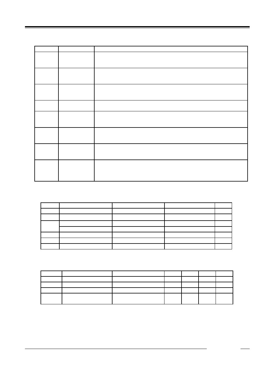
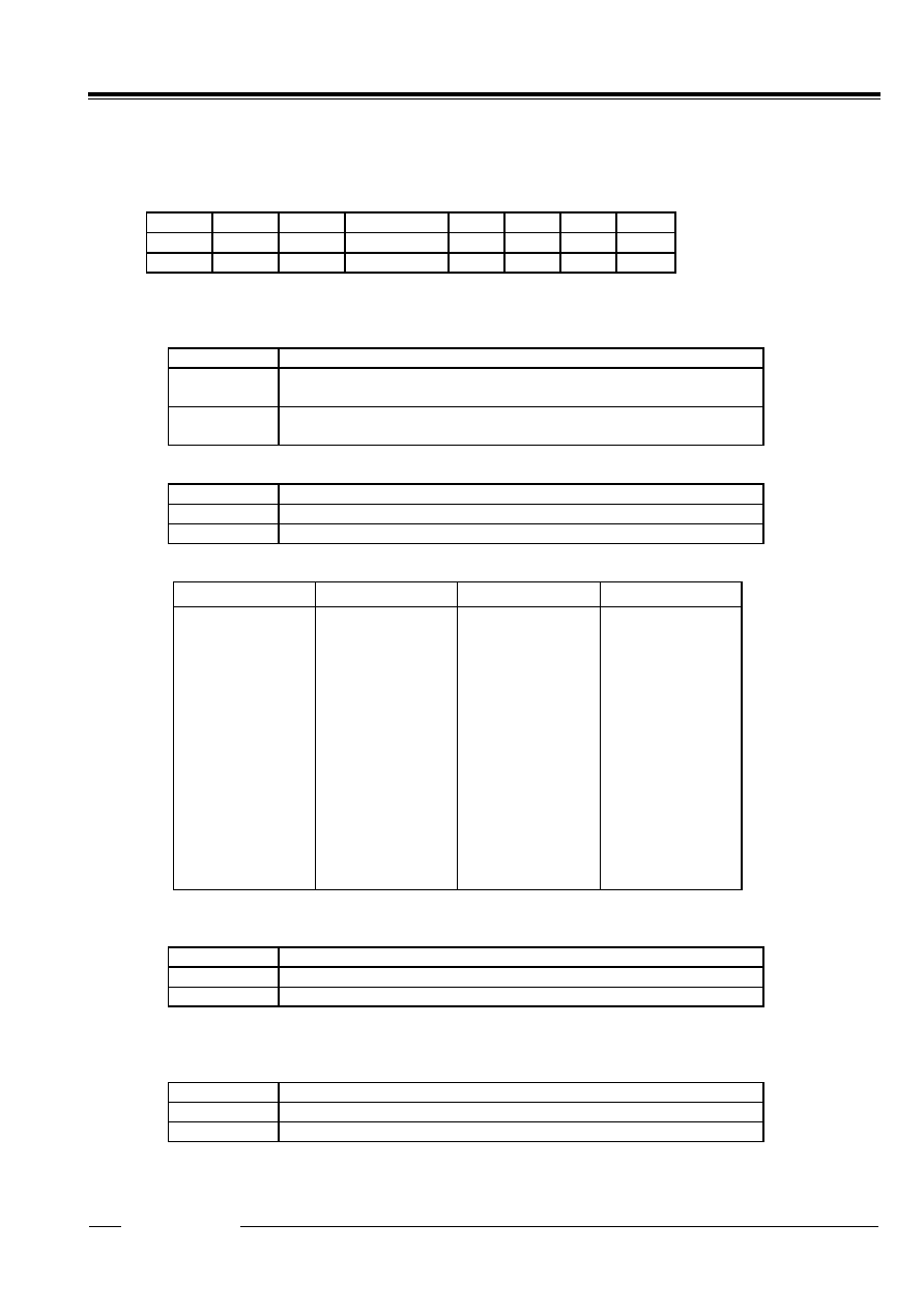
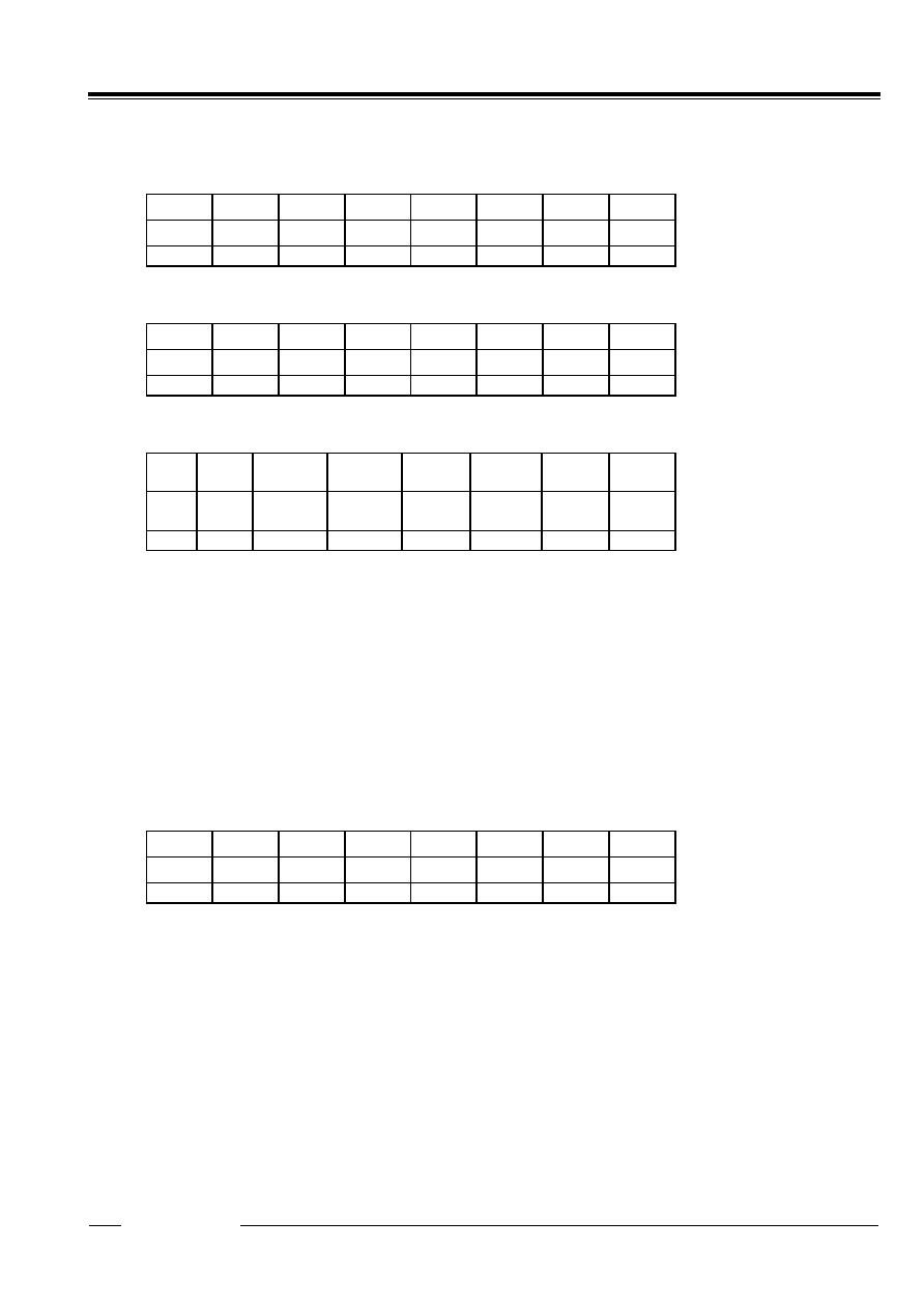
5. PIN DESCRIPTION
Symbol
Item
Description
SCL
Serial
Clock Line
The SCL pin is used to input clock pulses synchronizing the input and output
of data to and from the SDA pin. Allows a maximum input voltage of 5.5
volts regardless of supply voltage.
SDA
Serial
Data Line
The SDA pin is used to input or output data intended for writing or reading in
synchronization with the SCL pin. Up to 5.5v beyond VDD may be input.
This pin functions as an Nch open drain output.
/INTRA
Interrupt
Output A
The /INTRA pin is used to output periodic interrupt signals to the CPU and
alarm interrupt (Alarm_D) signals. Disabled at power-on from 0 volts. Nch.
open drain output.
/INTRB
Interrupt
Output B
The /INTRB pin is used to output alarm interrupt (Alarrm_W) signals to the
CPU. Disabled at power-on from 0 volts. Nch. open drain output.
32KOUT
32kHz Clock
Output
The 32KOUT pin is used to output 32.768-kHz clock pulses. Enabled at
power-on from 0 volts. CMOS output. The output is disabled if the CLKC pin
is set to Low or open.
CLKC
Clock control
input
The CLKC pin is used to control output of the 32KOUT pin. The clock output
is disabled and held low when the pin is set to low or open. Incorporates a
pull-down resistor.
OSCIN
OSCOUT
Oscillation
Circuit
Input / Output
The OSCIN and OSCOUT pins are used to connect the 32.768-kHz crystal
oscillator (with all other oscillation circuit components built into the
RV5C386A).
VDD
VSS
Positive Power
Supply Input
Negative Power
Supply Input
The VDD pin is connected to the power supply.
The VSS pin is grounded.
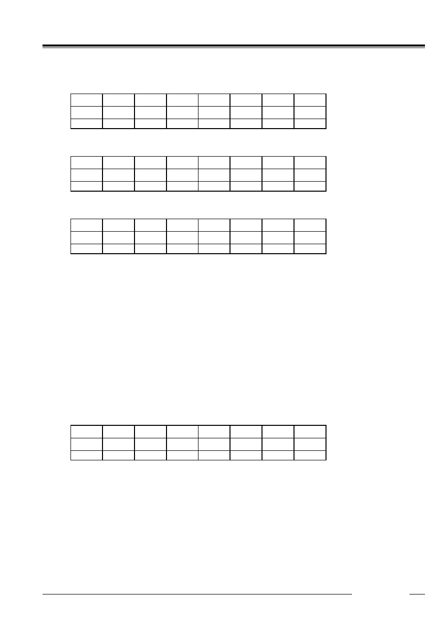
6. ABSOLUTE MAXIMUM RATINGS
(VSS=0V)
Symbol
Item
Pin Name
Description
Unit
VDD
Supply Voltage
-0.3 to +6.5
V
VI
Input Voltage
SCL, SDA, CLKC
-0.3 to +6.5
V
Output Voltage 1
SDA, /INTRA, /INTRB
-0.3 to +6.5
V
VO
Output Voltage 1
32KOUT
-0.3 to VDD+0.3
V
PD
Power Dissipation
Topt = 25
∞
C
300
mW
Topt
Operating Temperature
-40 to +85
∞
C
Tstg
Storage Temperature
-55 to +125
∞
C
7. RECOMMENDED OPERATING CONDITIONS
(VSS=0V, Topt=-40 to +85
∞
C)
Symbol
Item
Pin Name
Min,
Typ.
Max.
Unit
VDD
Supply Voltage
2.0
5.5
V
VCLK
Timekeeping Voltage
1.45
5.5
V
fXT
Oscillation Frequency
32.768
kHz
VPUP
Pull-up Voltage
SCL, SDA, /INTRA,
/INTRB
5.5
V

RV5C386A PRELIMINARY
12345
- 4 -
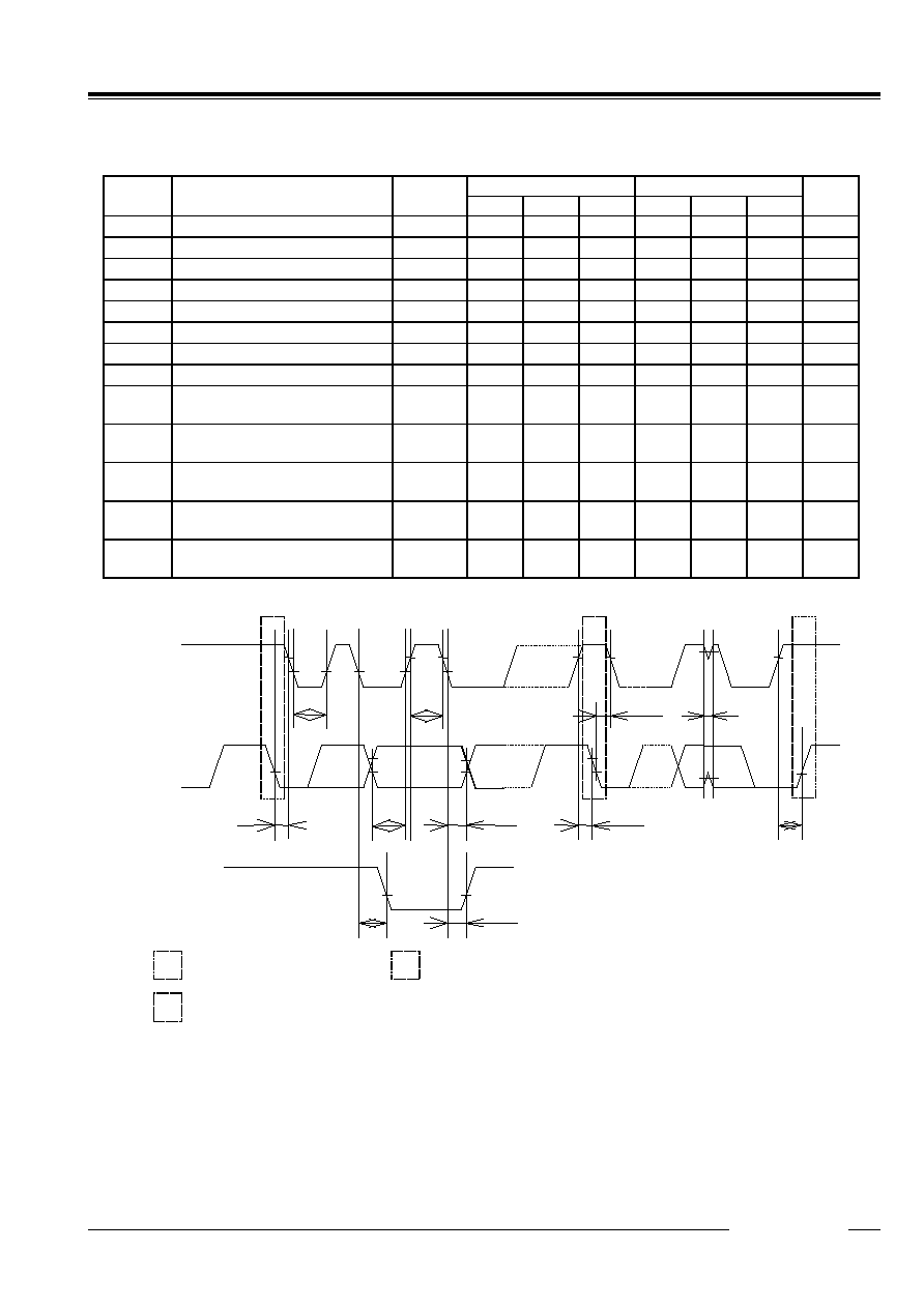
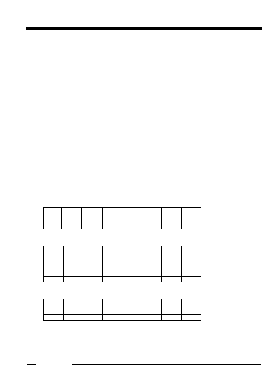
8. DC ELECTRICAL CHARACTERISTICS
(Unless otherwise specified : VSS=0V,VDD=3V,Topt=-40 to +85
∞
C)
Symbol
Item
Pin Name
Conditions
Min.
Typ.
Max.
Unit
VIH
"H" Input Voltage
0.8VDD
5.5
VIL
"L" Input Voltage
SCL,SDA,
CLKC
VDD=2.0 to 5.5V
-0.3
0.2VDD
V
IOH
"H" Output
Current
32KOUT
VOH=VDD-0.5V
-0.5mA
mA
IOL1
32KOUT
0.5
IOL2
/INTRA,
/INTRB
1.0
IOL3
"L" Output
Current
SDA
VOL=0.4V
4.0
mA
IIL
Input Leakage
Current
SCL
VI=5.5V or VSS
VDD=5.5V
-1
1
µ
A
ICLKC
Pull Down
Resistance Input
Current
CLKC
VI=5.5V
0.35
1.0
µ
A
IOZ
Output Off-state
Current
SDA,
/INTRA,
/INTRB
VO=5.5V or VSS
VDD=5.5V
-1
1
µ
A
IDD
Time Keeping
Current
VDD
VDD=3V,
SCL=SDA=3V,
CLKC=VSS
Output = OPEN
*1)
0.35
0.8
µ
A
VDETH
Supply Voltage
Monitoring
Voltage "H"
VDD
Topt=-30 to +70
∞
C
1.90
2.10
2.30
V
VDETL
Supply Voltage
Monitoring
Voltage "L"
VDD
Topt=-30 to +70
∞
C
1.45
1.60
1.80
V
CG
Internal
Oscillation
Capacitance 1
OSCIN
12
CD
Internal
Oscillation
Capacitance 2
OSCOUT
12
pF
*1) For Standby Current for outputting 32.768kHz clock pulses from the 32KOUT pin, see, "14.7 Typical
Characteristics".
PRELIMINARY RV5C386A
12345
- 5 -
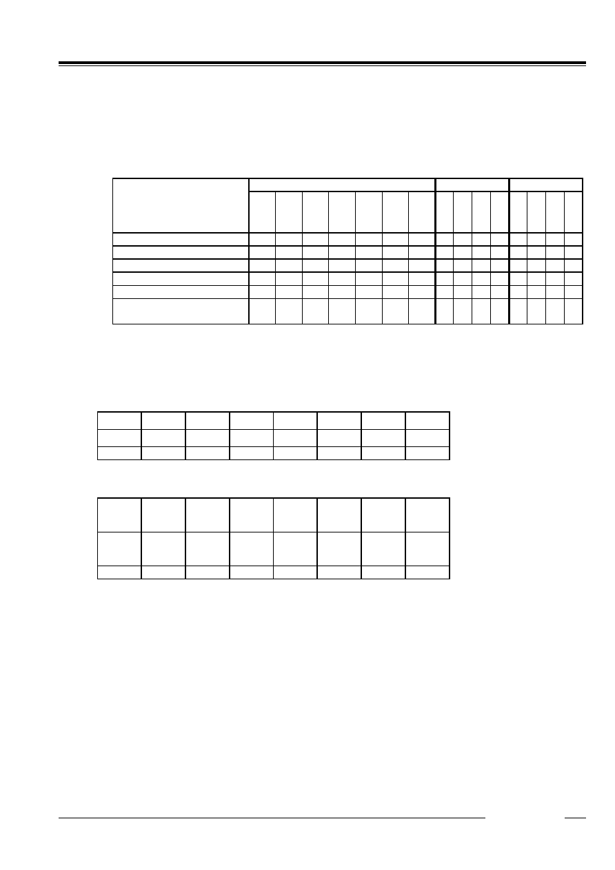
9. AC ELECTRICAL CHARACTERISTICS
Unless otherwise specified : VSS=0V,Topt=-40 to +85
∞
C
Input and Output Conditions : VIH=0.8
◊
VDD,VIL=0.2
◊
VDD,VOH=0.8
◊
VDD,VOL=0.2
◊
VDD,CL=50pF
VDD
2.0V
VDD
2.5V
Symbol
Item
Condi-
tions
Min.
Typ.
Max.
Min.
Typ.
Max.
Unit
f
SCL
SCL Clock Frequency
100
400
KHz
t
LOW
SCL Clock Low Time
4.7
1.3
µ
s
t
HIGH
SCL Clock High Time
4.0
0.6
µ
s
t
HD;STA
Start Condition Hold Time
4.0
0.6
µ
s
t
SU;STO
Stop Condition Set Up Time
4.0
0.6
µ
s
t
SU;STA
Start Condition Set Up Time
4.7
0.6
µ
s
t
SU;DAT
Data Set Up Time
250
200
ns
t
HD;DAT
Data Hold Time
0
0
ns
t
PL;DAT
SDA "L" Stable Time
After Falling of SCL
2.0
0.9
µ
s
t
PZ;DAT
SDA off Stable Time
After Falling of SCL
2.0
0.9
µ
s
t
R
Rising Time of SCL and
SDA (input)
1000
300
ns
t
F
Falling Time of SCL and
SDA (input)
300
300
ns
t
SP
Spike Width that can be
removed with Input Filter
50
50
ns
SDA(OUT)
SCL
S
Sr
P
t
PZ;DAT
t
HIGH
t
SU;DAT
t
HD;STA
t
SP
t
SU;STO
t
LOW
t
SU;STA
SDA(IN)
t
HD;STA
t
PL;DAT
Sr
P
Stop Condition
S
Start Condition
Repeated Start Condition
t
HD;DAT
RV5C386A PRELIMINARY
12345
- 6 -
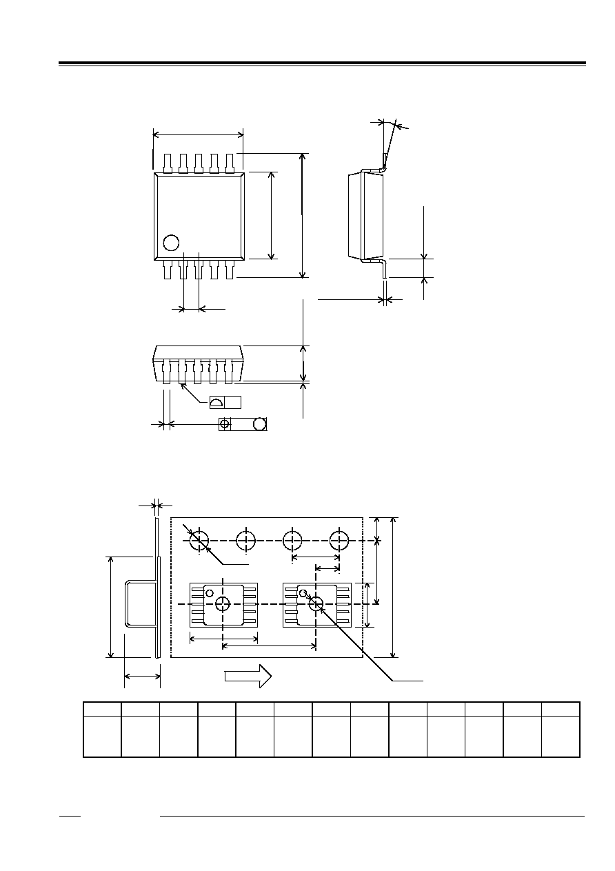
10. PACKAGE DIMENSIONS
(Unit : mm)
RV5C386A (SSOP10G)
M
2.8
±
0.2
0 to 10
∞
2.9
-0.1
5
10
1
+0.3
0.15
0.127
-0.05
4.0
±
0.3
0.1
0.2
±
0.1
+0.1
0.5
1.1
±
0.1
0.1
-0.05
+0.1
6
0.55
±
0.2
11. TAPING SPECIFICATION
The RV5C386A has one designated taping direction. The product designation for the taping components is
"RV5C386A-E2".
W
1
T
D
1
P
1
P
0
P
2
E
F
B
W
T
2
Pull-Out Directions
D
0
A
A
B
D
0
D
1
E
F
P
0
P
1
P
2
T
T
2
W
W
1
4.4
±
0.1
3.2
±
0.1
1.5
+0.1
-0
1.5
+0.1
-0
1.75
±
0.1
5.5
±
0.05
4.0
±
0.1
8.0
±
0.1
2.0
±
0.05
0.3
±
0.05
2.0
(MAX)
12.0
±
0.3
9.5
Unit:mm

PRELIMINARY RV5C386A
12345
- 7 -
12. GENERAL DESCRIPTION
(1) Interface with CPU
The RV5C386A is connected to the CPU by two signal lines SCL and SDA, through which it reads and writes
data from and to the CPU. Since the output of the I/O pin of SDA is open drain, data interfacing with a CPU
different supply voltage is possible by applying pull-up resistors on the circuit board. The maximum clock
frequency of 400kHz (at VDD
2.5V) of SCL enables data transfer in I
2
C-Bus fast mode.
(2) Clock and Calendar Function
The RV5C386A reads and writes time data from and to the CPU in units ranging from seconds to the last two
digits of the calendar year. The calendar year will automatically be identified as a leap year when its last two
digits are a multiple of 4. Also available is the 1900 / 2000 identification bit for Year 2000 compliance.
Consequently, leap years up to the year 2099 can automatically be identified as such.
*) The year 2000 is a leap year while the year 2100 is not a leap year.
(3) Alarm Function
The RV5C386A incorporates the alarm interrupt circuit configured to generate interrupt signals to the CPU at
preset times. The alarm interrupt circuit allows two types of alarm settings specified by the Alarm_W
registers and the Alarm_D registers. The Alarm_W registers allow week, hour, and minute alarm settings
including combinations of multiple day-of-week settings such as "Monday, Wednesday, and Friday" and
"Saturday and Sunday". The Alarm_D registers allow hour and minute alarm settings. The Alarm_W
outputs from /INTRB pin, and the Alarm_D outputs from /INTRA pin. The current /INTRA or /INTRB
conditions specified by the flag bits for each alarm function can be checked from the CPU by using a polling
function.
(4) High-precision Oscillation Adjustment Function
The RV5C386A has built-in oscillation stabilization capacitors (CG and CD), which can be connected to an
external crystal oscillator to configure an oscillation circuit. To correct deviations in the oscillation frequency
of the crystal oscillator, the oscillation adjustment circuit is configured to allow correction of a time count gain
or loss (up to
±
1.5 ppm at 25
∞
C) from the CPU within a maximum range of approximately + 189 ppm in
increments of approximately 3 ppm. Such oscillation frequency adjustment in each system has the following
advantages:
* Allows timekeeping with much higher precision than conventional RTCs while using a crystal oscillator with
a wide range of precision variations.
* Corrects seasonal frequency deviations through seasonal oscillation adjustment.
* Allows timekeeping with higher precision particularly with a temperature sensing function out of RTC,
through oscillation adjustment in tune with temperature fluctuations.
(5) Oscillation Halt Sensing Function and Supply Voltage Monitoring Function
The RV5C386A incorporates an oscillation halt sensing circuit equipped with internal registers configured to
record any past oscillation halt, thereby identifying whether they are powered on from 0 volts or battery
backed-up. As such, the oscillation halt sensing circuit is useful for judging the validity of time data.
The RV5C386A also incorporates a supply voltage monitoring circuit equipped with internal registers
configured to record any drop in supply voltage below a certain threshold value. Supply voltage monitoring
threshold settings can be selected between 2.1 and 1.6 volts through internal register settings. The
oscillation halt sensing circuit is configured to confirm the established invalidation of time data in contrast to
the supply voltage monitoring circuit intended to confirm the potential invalidation of time data. Further, the
supply voltage monitoring circuit can be applied to battery supply voltage monitoring.

RV5C386A PRELIMINARY
12345
- 8 -
(6) Periodic Interrupt Function
The RV5C386A incorporates the periodic interrupt circuit configured to generate periodic interrupt signals
aside from interrupt signals generated by the alarm interrupt circuit for output from the /INTRA pin. Periodic
interrupt signals have five selectable frequency settings of 2 Hz (once per 0.5 seconds), 1 Hz (once per 1
second), 1/60 Hz (once per 1 minute), 1/3600 Hz (once per 1 hour), and monthly (the first day of every month).
Further, periodic interrupt signals also have two selectable waveforms, a normal pulse form (with a frequency
of 2 Hz or 1 Hz) and special form adapted to interruption from the CPU in the level mode (with second,
minute, hour, and month interrupts). The condition of periodic interrupt signals can be monitored by using a
polling function.
(7) 32kHz Clock Output
The RV5C386A incorporates a 32-kHz clock circuit configured to generate clock pulses with the oscillation
frequency of a 32.768kHz crystal oscillator for output from the 32KOUT pin (CMOS push-pull output). The
32-kHz clock output is enabled and disabled when the CLKC pin is held high, and low or open, respectively.

PRELIMINARY RV5C386A
12345
- 9 -
13.
FUNCTION DESCRIPTIONS
13.1.
Address Mapping
Address Register Name
D a t a
A3A2A1A0
D7
D6
D5
D4
D3
D2
D1
D0
0
0 0 0 0
Second Counter
-
*2)
S40
S20
S10
S8
S4
S2
S1
1
0 0 0 1
Minute Counter
-
M40
M20
M10
M8
M4
M2
M1
2
0 0 1 0
Hour Counter
-
-
H20
P
/A
H10
H8
H4
H2
H1
3
0 0 1 1
Day-of-week Counter
-
-
-
-
-
W4
W2
W1
4
0 1 0 0
Day-of-month Counter
-
-
D20
D10
D8
D4
D2
D1
5
0 1 0 1
Month Counter and
Century Bit
/19
20
-
-
MO10
MO8
MO4
MO2
MO1
6
0 1 1 0
Year Counter
Y80
Y40
Y20
Y10
Y8
Y4
Y2
Y1
7
0 1 1 1
Oscillation Adjustment
Register *3)
-
F6
F5
F4
F3
F2
F1
F0
8
1 0 0 0
Alarm_W
(Minute Register)
-
WM40 WM20
WM10
WM8
WM4
WM2
WM1
9
1 0 0 1
Alarm_W
(Hour Register)
-
-
WH20
WP
/A
WH10
WH8
WH4
WH2
WH1
A
1 0 1 0
Alarm_W
(Day-of-week Register)
-
WW6
WW5
WW4
WW3
WW2
WW1
WW0
B
1 0 1 1
Alarm_D
(Minute Register)
-
DM40
DM20
DM10
DM8
DM4
DM2
DM1
C
1 1 0 0
Alarm_D
(Hour Register)
-
-
DH20
DP
/A
DH10
DH8
DH4
DH2
DH1
D
1 1 0 1
-
-
-
-
-
-
-
-
E
1 1 1 0
Control Register 1 *3)
WALE DALE
/12
24
SCRA-
TCH3
TEST
CT2
CT1
CT0
F
1 1 1 1
Control Register 2 *3)
VDSL VDET
SCRA-
TCH1
XSTP
SCRA-
TCH2
CTFG WAFG DAFG
Notes:
* 1) All the data listed above accept both reading and writing.
* 2) The data marked with "-" is invalid for writing and reset to 0 for reading.
* 3) When the XSTP bit is set to 1 in Control Register 2, all the bits are reset to 0 in Oscillation Adjustment
Register, Control Register 1 and Control Register 2 excluding the XSTP bit.
RV5C386A PRELIMINARY
12345
- 10 -
13.2.
Register Settings
13.2.1. Control Register 1 (ADDRESS Eh)
D7
D6
D5
D4
D3
D2
D1
D0
WALE
DALE
/12
24
SCRATCH3
TEST
CT2
CT1
CT0
(For Writing)
WALE
DALE
/12
24
SCRATCH3
TEST
CT2
CT1
CT0
(For Reading)
0
0
0
0
0
0
0
0
Default Settings *)
*) Default settings: Default value means read/written values when the XSTP bit is set to "1" due to power-on
from 0 volts or supply voltage drop.
(1)
WALE, DALE
Alarm_W Enable Bit, Alarm_D Enable Bit
WALE,DALE
Description
0
Disabling the alarm interrupt circuit (under the control of the settings
of the Alarm_W registers and the Alarm_D registers).
(Default)
1
Enabling the alarm interrupt circuit (under the control of the settings
of the Alarm_W registers and the Alarm_D registers)
(2)
/12
24
12-/24-hour Mode Selection Bit
/12
24
Description
0
Selecting the 12-hour mode with a.m. and p.m. indications.
(Default)
1
Selecting the 24-hour mode
Setting the /12
24 bit to 0 and 1 specifies the 12-hour mode and the 24-hour mode, respectively.
24-hour mode
12-hour mode
24-hour mode
12-hour mode
00
12 (AM12)
12
32 (PM12)
01
01 (AM 1)
13
21 (PM 1)
02
02 (AM 2)
14
22 (PM 2)
03
03 (AM 3)
15
23 (PM 3)
04
04 (AM 4)
16
24 (PM 4)
05
05 (AM 5)
17
25 (PM 5)
06
06 (AM 6)
18
26 (PM 6)
07
07 (AM 7)
19
27 (PM 7)
08
08 (AM 8)
20
28 (PM 8)
09
09 (AM 9)
21
29 (PM 9)
10
10 (AM10)
22
30 (PM10)
11
11 (AM11)
23
31 (PM11)
Setting the /12
24 bit should precede writing time data
(3) SCRATCH3
Scratch Bit 3
SCRATCH3
Description
0
(Default)
1
The SCRATCH3 bit is intended for scratching and accepts the reading and writing of 0 and 1. The SCRATCH3
bit will be set to 0 when the XSTP bit is set to 1 in the Control Register 2.
(4) TEST
Test Bit
TEST
Description
0
Normal operation mode.
(Default)
1
Test mode.
The TEST bit is used only for testing in the factory and should normally be set to 0.
PRELIMINARY RV5C386A
12345
- 11 -
(5) CT2,CT1, and CT0
Periodic Interrupt Selection Bits
Description
CT2
CT1
CT0
Wave form mode
Interrupt Cycle and Falling Timing
0
0
0
-
OFF(H)
(Default)
0
0
1
-
Fixed at "L"
0
1
0
Pulse Mode *1)
2Hz(Duty50%)
0
1
1
Pulse Mode *1)
1Hz(Duty50%)
1
0
0
Level Mode *2)
Once per 1 second (Synchronized with
second counter increment)
1
0
1
Level Mode *2)
Once per 1 minute (at 00 seconds of every
minute)
1
1
0
Level Mode *2)
Once per hour (at 00 minutes and 00
seconds of every hour)
1
1
1
Level Mode *2)
Once per month (at 00 hours, 00 minutes,
and 00 seconds of first day of every month)
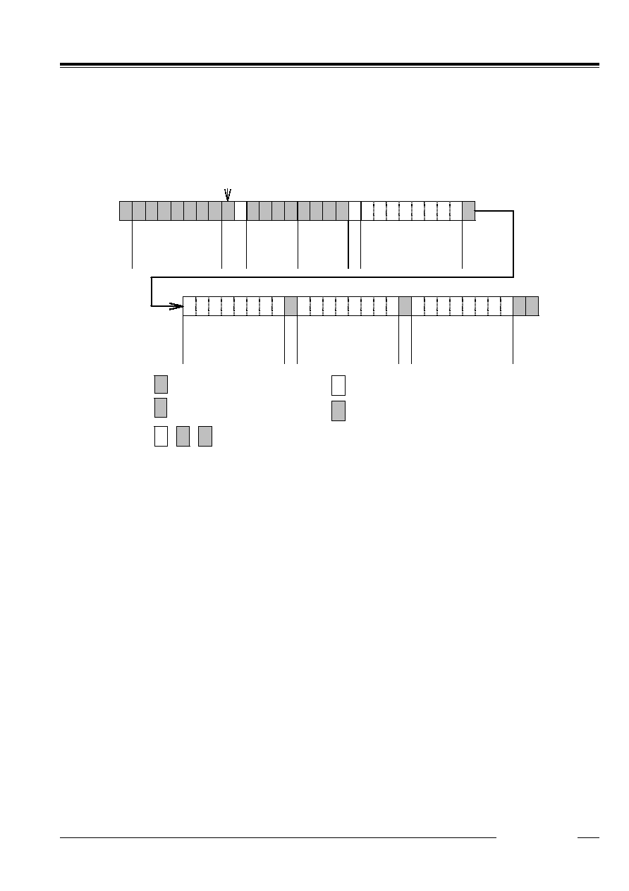
*1) Pulse Mode: 2-Hz and 1-Hz clock pulses are output in synchronization with the increment of the second
counter as illustrated in the timing chart below.
/INTRA Pin
Rewriting of the second counter
CTFG Bit
Approx. 92
µ
s
(Increment of second counter)
In the pulse mode, the increment of the second counter is delayed by approximately 92
µ
s from the falling edge of
clock pulses. Consequently, time readings immediately after the falling edge of clock pulses may appear to lag
behind the time counts of the real-time clocks by approximately 1 second. Rewriting the second counter will
reset the other time counters of less than 1 second, driving the /INTRA pin low.
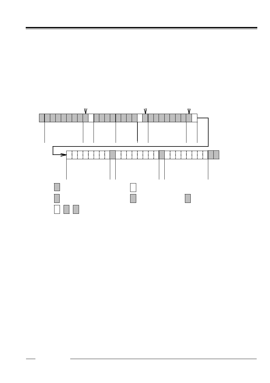
*2) Level Mode: Periodic interrupt signals are output with selectable interrupt cycle settings of 1 second, 1
minute, 1 hour, and 1 month. The increment of the second counter is synchronized with the
falling edge of periodic interrupt signals. For example, periodic interrupt signals with an
interrupt cycle setting of 1 second are output in synchronization with the increment of the second
counter as illustrated in the timing chart below.
/INTRA Pin
(Increment of
second counter)
CTFG Bit
Setting CTFG bit to 0
Setting CTFG bit to 0
(Increment of
second counter)
(Increment of
second counter)
*1), *2) When the oscillation adjustment circuit is used, the interrupt cycle will fluctuate once per 20sec. as follows:
Pulse Mode: The "L" period of output pulses will increment or decrement by a maximum of
±
3.784 ms. For
example, 1-Hz clock pulses will have a duty cycle of 50
±
0.3784%.
Level Mode: A periodic interrupt cycle of 1 second will increment or decrement by a maximum of
±
3.784 ms.
RV5C386A PRELIMINARY
12345
- 12 -
13.2.2. Control Register 2 (Address Fh)
D7
D6
D5
D4
D3
D2
D1
D0
VDSL
VDET
SCRA-
TCH1
XSTP SCRA-
TCH2
CTFG
WAFG DAFG
(For Writing)
VDSL
VDET
SCRA-
TCH1
XSTP
SCRA-
TCH2
CTFG
WAFG DAFG
(For Reading)
0
0
0
1
0
0
0
0
Default Settings *)
*) Default settings: Default value means read / written values when the XSTP bit is reset due to power-on from
0 volts or supply voltage drop.
(1) VDSL
Supply Voltage Monitoring Threshold Selection Bit
VDSL
Description
0
Selecting the supply voltage monitoring threshold setting of 2.1v.
(Default)
1
Selecting the supply voltage monitoring threshold setting of 1.6v.
The VDSL bit is intended to select the supply voltage monitoring threshold settings.
(2)
VDET
Supply Voltage Monitoring Result Indication Bit
VDET
Description
0
Indicating supply voltage above the supply voltage monitoring
threshold settings.
(Default)
1
Indicating supply voltage below the supply voltage monitoring
threshold settings.
Once the VDET bit is set to 1, the supply voltage monitoring circuit will be disabled while the VDET bit will hold the
setting of 1. The VDET bit accepts only the writing of 0, which restarts the supply voltage monitoring circuit.
Conversely, setting the VDET bit to 1 causes no event.
(3) SCRATCH1
Scratch Bit 1
SCRATCH1
Description
0
(Default)
1
The SCRATCH1 bit is intended for scratching and accepts the reading and writing of 0 and 1. The SCRATCH1
bit will be set to 0 when the XSTP bit is set to 1 in the Control Register 2.
(4) XSTP
Oscillation Halt Sensing Bit
XSTP
Description
0
Sensing a normal condition of oscillation
1
Sensing a halt of oscillation
(Default)
The XSTP bit is for sensing a halt in the oscillation of the crystal oscillator.
*
The XSTP bit will be set to 1 once a halt in the oscillation of the crystal oscillator is caused by such events as
power-on from 0 volts and a drop in supply voltage. The XSTP bit will hold the setting of 1 even after the
restart of oscillation. As such, the XSTP bit can be applied to judge the validity of clock and calendar data
after power-on or a drop in supply voltage.
*
When the XSTP bit is set to 1, all bits will be reset to 0 in the Oscillation Adjustment Register, Control Register
1, and Control Register 2, stopping the output from /INTRA and /INTRB pins and starting the output of
32.768-kHz clock pulses from the 32KOUT pin.
*
The XSTP bit accepts only the writing of 0, which restarts the oscillation halt sensing circuit. Conversely,
setting the XSTP bit to 1 causes no event.
*
It is recommendable to frequently check the XSTP bit for setting errors or data garbles, which may seriously
affect the operation of the RV5C386A.
PRELIMINARY RV5C386A
12345
- 13 -
(5) SCRATCH2
Scratch Bit 2
SCRATCH2
Description
0
(Default)
1
The SCRATCH2 bit is intended for scratching and accepts the reading and writing of 0 and 1. The SCRATCH2
bit will be set to 0 when the XSTP bit is set to 1 in the Control Register 2.
(6) CTFG
Periodic Interrupt Flag Bit
CTFG
Description
0
Periodic interrupt output = "H"
(Default)
1
Periodic interrupt output = "L"
The CTFG bit is set to 1 when the periodic interrupt signals are output from the /INTRA pin ("L"). The CTFG bit
accepts only the writing of 0 in the level mode, which disables ("H") the /INTRA pin until it is enabled ("L") again in
the next interrupt cycle. Conversely, setting the CTFG bit to 1 causes no event.
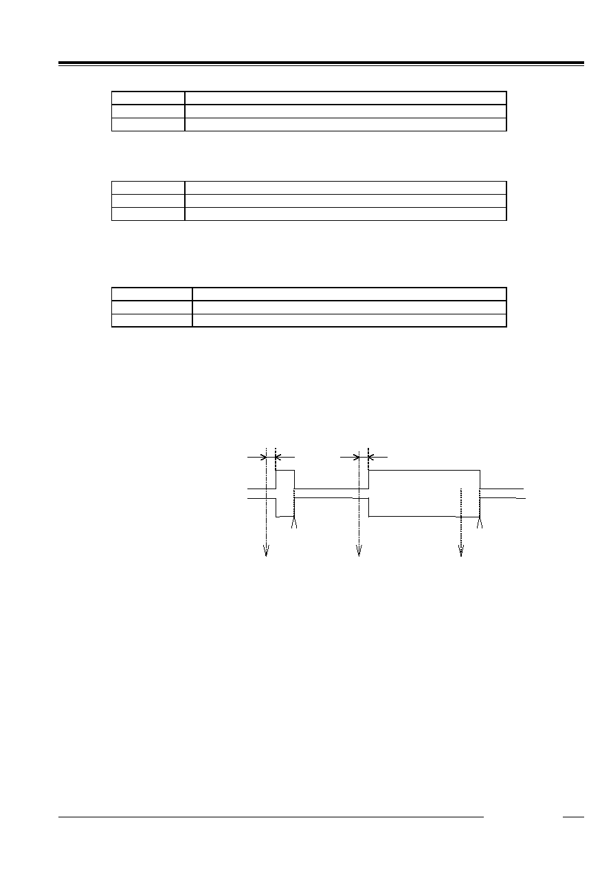
(7) WAFG,DAFG Alarm_W Flag Bit and Alarm_D Flag Bit
WAFG,DAFG
Description
0
Indicating a mismatch between current time and preset alarm time
(Default)
1
Indicating a match between current time and preset alarm time
The WAFG and DAFG bits are valid only when the WALE and DALE have the setting of 1, which is caused
approximately 61
µ
s after any match between current time and preset alarm time specified by the Alarm_W
registers and the Alarm_D registers. The WAFG (DAFG) bit accepts only the writing of 0. /INTRB (/INTRA) pin
outputs off ("H") when this bit is set to 0. And /INTRB (/INTRA) pin outputs "L" again at the next preset alarm
time. Conversely, setting the WAFG and DAFG bits to 1 causes no event. The WAFG and DAFG bits will have
the reading of 0 when the alarm interrupt circuit is disabled with the WALE and DALE bits set to 0. The settings
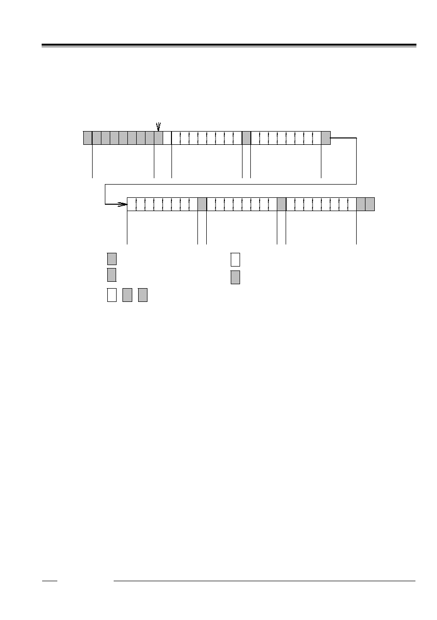
of the WAFG and DAFG bits are synchronized with the output of the /INTRB (/INTRA) pin as shown in the timing
chart below.
/INTRB(/INTRA) Pin
Writing of 0 to
WAFG(DAFG) bit
WAFG(DAFG) Bit
(Match between
current time and
preset alarm time)
Approx. 61
µ
s
Approx. 61
µ
s
Writing of 0 to
WAFG(DAFG) bit
(Match between
current time and
preset alarm time)
(Match between
current time and
preset alarm time)
RV5C386A PRELIMINARY
12345
- 14 -
13.2.3. Time Counter (Address 0-2h)
∑
Second Counter (Address 0h)
D7
D6
D5
D4
D3
D2
D1
D0
-
S40
S20
S10
S8
S4
S2
S1
(For Writing)
0
S40
S20
S10
S8
S4
S2
S1
(For Reading)
0
Indefinite
Indefinite
Indefinite
Indefinite
Indefinite
Indefinite
Indefinite
Default Settings *)
∑
Minute Counter (Address 1h)
D7
D6
D5
D4
D3
D2
D1
D0
-
M40
M20
M10
M8
M4
M2
M1
(For Writing)
0
M40
M20
M10
M8
M4
M2
M1
(For Reading)
0
Indefinite
Indefinite
Indefinite
Indefinite
Indefinite
Indefinite
Indefinite
Default Settings *)
∑
Hour Counter (Address 2h)
D7
D6
D5
D4
D3
D2
D1
D0
-
-
P
/A
or H20
H10
H8
H4
H2
H1
(For Writing)
0
0
P
/A
or H20
H10
H8
H4
H2
H1
(For Reading)
0
0
Indefinite
Indefinite
Indefinite
Indefinite
Indefinite
Indefinite
Default Settings *)
*) Default settings: Default value means read/written values when the XSTP bit is set to "1" due to power-on
from 0 volts or supply voltage drop.
*
Time digit display (BCD format) as follows:
The second digits range from 00 to 59 and are carried to the minute digit in transition from 59 to 00.
The minute digits range from 00 to 59 and are carried to the hour digits in transition from 59 to 00.
The hour digits range as shown in "13.2.1. ≠ (2). /12
24: 12-/24-hour Mode Selection Bit" and are carried to
the day-of-month and day-of-week digits in transition from PM11 to AM12 or from 23 to 00.
*
Any writing to the second counter resets divider units of less than 1 second.
*
Any carry from lower digits with the writing of non-existent time may cause the time counters to malfunction.
Therefore, such incorrect writing should be replaced with the writing of existent time data.
13.2.4. Day-of-week Counter (Address 3h)
D7
D6
D5
D4
D3
D2
D1
D0
-
-
-
-
-
W4
W2
W1
(For Writing)
0
0
0
0
0
W4
W2
W1
(For Reading)
0
0
0
0
0
Indefinite
Indefinite
Indefinite
Default Settings *)
*) Default settings: Default value means read/written values when the XSTP bit is set to "1" due to power-on
from 0 volts or supply voltage drop.
* The day-of-week counter is incremented by 1 when the day-of-week digits are carried to the day-of-
month digits.
* Day-of-week display (incremented in septimal notation):
(W4, W2, W1) = (0, 0, 0)
(0, 0, 1)
...
(1, 1, 0)
(0, 0, 0)
* Correspondences between days of the week and the day-of-week digits are user-definable
(e.g. Sunday = 0, 0, 0)
* The writing of (1, 1, 1) to (W4, W2, W1) is prohibited except when days of the week are unused.
PRELIMINARY RV5C386A
12345
- 15 -
13.2.5. Calendar Counter (Address 4-6h)
∑
Day-of-month Counter (Address 4h)
D7
D6
D5
D4
D3
D2
D1
D0
-
-
D20
D10
D8
D4
D2
D1
(For Writing)
0
0
D20
D10
D8
D4
D2
D1
(For Reading)
0
0
Indefinite
Indefinite
Indefinite
Indefinite
Indefinite
Indefinite
Default Settings *)
∑
Month Counter + Century Bit (Address 5h)
D7
D6
D5
D4
D3
D2
D1
D0
/19
20
-
-
MO10
MO8
MO4
MO2
MO1
(For Writing)
/19
20
0
0
MO10
MO8
MO4
MO2
MO1
(For Reading)
Indefinite
0
0
Indefinite
Indefinite
Indefinite
Indefinite
Indefinite
Default Settings *)
∑
Year Counter (Address 6h)
D7
D6
D5
D4
D3
D2
D1
D0
Y80
Y40
Y20
Y10
Y8
Y4
Y2
Y1
(For Writing)
Y80
Y40
Y20
Y10
Y8
Y4
Y2
Y1
(For Reading)
Indefinite
Indefinite
Indefinite
Indefinite
Indefinite
Indefinite
Indefinite
Indefinite
Default Settings *)
*) Default settings: Default value means read/written values when the XSTP bit is set to "1" due to power-on
from 0 volts or supply voltage drop.
* The calendar counters are configured to display the calendar digits in BCD format by using the automatic
calendar function as follows:
The day-of-month digits (D20 to D1) range from 1 to 31 for January, March, May, July, August, October, and
December; from 1 to 30 for April, June, September, and November; from 1 to 29 for February in leap years;
from 1 to 28 for February in ordinary years. The day-of-month digits are carried to the month digits in
reversion from the last day of the month to 1. The month digits (MO10 to MO1) range from 1 to 12 and are
carried to the year digits in reversion from 12 to 1.
The year digits (Y80 to Y1) range from 00 to 99 (00, 04, 08,
...
, 92, and 96 in leap years) and are carried to the
/19
20 digits in reversion from 99 to 00.
The /19
20 digits cycle between 0 and 1 in reversion from 99 to 00 in the year digits.
* Any carry from lower digits with the writing of non-existent calendar data may cause the calendar counters to
malfunction. Therefore, such incorrect writing should be replaced with the writing of existent calendar data.
13.2.6. Oscillation Adjustment Register (Address 7h)
D7
D6
D5
D4
D3
D2
D1
D0
-
F6
F5
F4
F3
F2
F1
F0
(For Writing)
0
F6
F5
F4
F3
F2
F1
F0
(For Reading)
0
0
0
0
0
0
0
0
Default Settings *)
*) Default settings: Default value means read/written values when the XSTP bit is set to "1" due to power-on
from 0 volts or supply voltage drop.
RV5C386A PRELIMINARY
12345
- 16 -
F6 to F0 bits
The Oscillation Adjustment Circuit is configured to change time counts of 1 second on the basis of the settings
of
the Oscillation Adjustment Register when the second digits read 00, 20, or 40 seconds. Normally, the Second
Counter is incremented once per 32768 32.768-kHz clock pulses generated by the crystal oscillator. Writing to
the F6 to F0 bits activates the oscillation adjustment circuit.
* The Oscillation Adjustment Circuit will not operate with the same
timing (00, 20, or 40 seconds)
as the timing of writing to the Oscillation Adjustment Register.
* The F6 bit setting of 0 causes an increment of time counts by ((F5, F4, F3, F2, F1, F0) - 1) x 2.
The F6 bit setting of 1 causes a decrement of time counts by ((/F5, /F4, /F3, /F2, /F1, /F0) + 1) x 2.
The settings of "*, 0, 0, 0, 0, 0, *" ("*" representing either "0" or "1") in the F6, F5, F4, F3, F2, F1, and F0
bits cause neither an increment nor decrement of time counts.
Example:
When the second digits read 00, 20, or 40, the settings of "0, 0, 0, 0, 1, 1, 1" in the F6, F5, F4, F3, F2, F1, and F0
bits cause an increment of the current time counts of 32768 by (7 - 1) x 2 to 32780 (a current time count loss).
When the second digits read 00, 20, or 40, the settings of "0, 0, 0, 0, 0, 0, 1" in the F6, F5, F4, F3, F2, F1, and F0
bits cause neither an increment nor a decrement of the current time counts of 32768.
When the second digits read 00, 20, or 40, the settings of "1, 1, 1, 1, 1, 1, 0" in the F6, F5, F4, F3, F2, F1, and F0
bits cause a decrement of the current time counts of 32768 by (- 2) x 2 to 32764 (a current time count gain).
An increase of two clock pulses once per 20 seconds causes a time count loss of approximately 3 ppm (2 / (32768
x 20 = 3.051 ppm). Conversely, a decrease of two clock pulses once per 20 seconds causes a time count gain of
3 ppm. Consequently, deviations in time counts can be corrected with a precision of
±
1.5 ppm. Note that the
oscillation adjustment circuit is configured to correct deviations in time counts and not the oscillation frequency of
the 32.768-kHz clock pulses. For further details, see "14. 2. 4. Oscillation Adjustment Circuit".
13.2.7. Alarm_W Registers (Address 8-Ah)
∑
Alarm_W Minute Register (Address 8h)
D7
D6
D5
D4
D3
D2
D1
D0
-
WM40
WM20
WM10
WM8
WM4
WM2
WM1
(For Writing)
0
WM40
WM20
WM10
WM8
WM4
WM2
WM1
(For Reading)
0
Indefinite
Indefinite
Indefinite
Indefinite
Indefinite
Indefinite
Indefinite
Default Settings *)
∑
Alarm_W Hour Register (Address 9h)
D7
D6
D5
D4
D3
D2
D1
D0
-
-
WH20
WP
/A
WH10
WH8
WH4
WH2
WH1
(For Writing)
0
0
WH20
WP
/A
WH10
WH8
WH4
WH2
WH1
(For Reading)
0
0
Indefinite
Indefinite
Indefinite
Indefinite
Indefinite
Indefinite
Default Settings *)
∑
Alarm_W Day-of-week Register (Address Ah)
D7
D6
D5
D4
D3
D2
D1
D0
-
WW6
WW5
WW4
WW3
WW2
WW1
WW0
(For Writing)
0
WW6
WW5
WW4
WW3
WW2
WW1
WW0
(For Reading)
0
Indefinite
Indefinite
Indefinite
Indefinite
Indefinite
Indefinite
Indefinite
Default Settings *)
*) Default settings: Default value means read/written values when the XSTP bit is set to "1" due to power-on
from 0 volts or supply voltage drop.
* The D5 bit of the Alarm_W Hour Register represents WP/A when the 12-hour mode is selected (0 for a.m. and
1 for p.m.)
and WH20 when the 24-hour mode is selected (tens in the hour digits)
.
* The Alarm_W Registers should not have any non-existent alarm time settings.
PRELIMINARY RV5C386A
12345
- 17 -
(Note that any mismatch between current time and preset alarm time specified by the Alarm_W registers may
disable the alarm interrupt circuit.)
* When the 12-hour mode is selected, the hour digits read 12 and 32 for 0 a.m. and 0 p.m., respectively.
(See "13.2. 1. ≠ (2). /12 * 24: 12-/24-hour Mode Selection Bit").
* WW0 to WW6 correspond to W4, W2, and W1 of the day-of-week counter with settings ranging from (0, 0, 0)
to (1, 1, 0).
* WW0 to WW6 with respective settings of 0 disable the outputs of the Alarm_W Registers.
Example of Alarm Time Setting
Alarm
Day-of-week
12-hour mode
24-hour mode
Preset alarm time
Sun.
Mon.
Tue.
Wed.
Th.
Fri.
Sat.
10
hr.
1
hr.
10
min.
1
min.
10
hr.
1
hr.
10
min.
1
min.
WW0 WW1 WW2 WW3 WW4 WW5 WW6
00:00 a.m. on all days
1
1
1
1
1
1
1
1
2
0
0
0
0
0
0
01:30 a.m. on all days
1
1
1
1
1
1
1
0
1
3
0
0
1
3
0
11:59 a.m. on all days
1
1
1
1
1
1
1
1
1
5
9
1
1
5
9
00:00 p.m. on Mon. to Fri.
0
1
1
1
1
1
0
3
2
0
0
1
2
0
0
01:30 p.m. on Sun.
1
0
0
0
0
0
0
2
1
3
0
1
3
3
0
11:59 p.m.
on Mon. ,Wed., and Fri.
0
1
0
1
0
1
0
3
1
5
9
2
3
5
9
Note that the correspondence between WW0 to WW6 and the days of the week shown in the above table is only
an example and not mandatory.
13.2.8. Alarm_D Register (Address B-Ch)
∑
Alarm_D Minute Register (Address Bh)
D7
D6
D5
D4
D3
D2
D1
D0
-
DM40
DM20
DM10
DM8
DM4
DM2
DM1
(For Writing)
0
DM40
DM20
DM10
DM8
DM4
DM2
DM1
(For Reading)
0
Indefinite
Indefinite
Indefinite
Indefinite
Indefinite
Indefinite
Indefinite
Default Settings *)
∑
Alarm_D Hour Register (Address Ch)
D7
D6
D5
D4
D3
D2
D1
D0
-
-
DH20
DP
/A
DH10
DH8
DH4
DH2
DH1
(For Writing)
0
0
DH20
DP
/A
DH10
DH8
DH4
DH2
DH1
(For Reading)
0
0
Indefinite
Indefinite
Indefinite
Indefinite
Indefinite
Indefinite
Default Settings *)
*) Default settings: Default value means read/written values when the XSTP bit is set to "1" due to power-on
from 0 volts or supply voltage drop.
*
The D5 bit represents DP/A when the 12-hour mode is selected (0 for a.m. and 1 for p.m.) and DH20 when the
24-hour mode is selected (tens in the hour digits).
* The Alarm_D registers should not have any non-existent alarm time settings.
(Note that any mismatch between current time and preset alarm time specified by the Alarm_D registers may
disable the alarm interrupt circuit.)
*
When the 12-hour mode is selected, the hour digits read 12 and 32 for 0a.m. and 0p.m., respectively.
(see "13.2.1. (2) /12 * 24: 12-/24-hour Mode Selection Bit").
RV5C386A PRELIMINARY
12345
- 18 -
14.
USAGE
14.1.
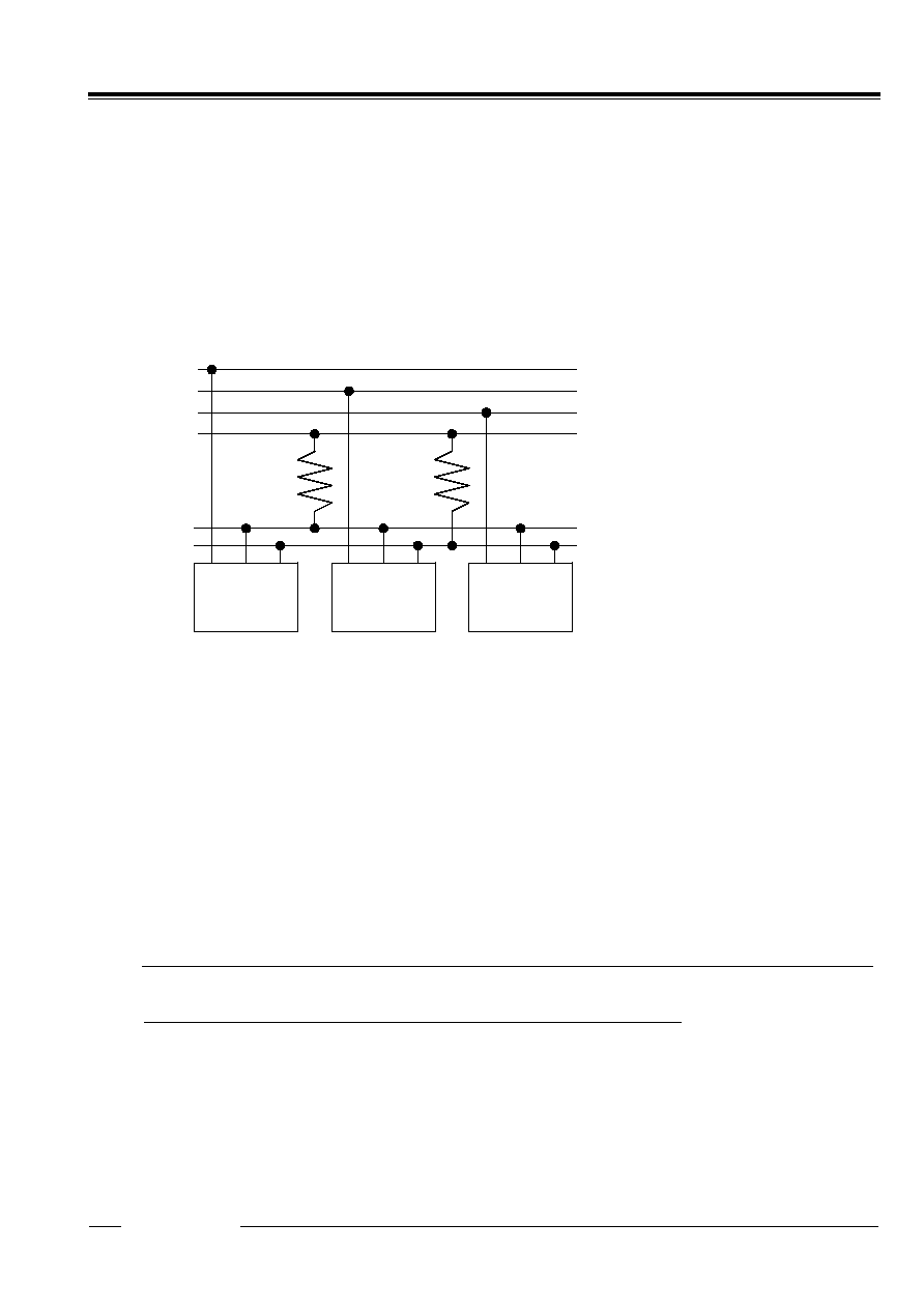
Interfacing with the CPU
The RV5C386A employs the I
2
C-Bus system to be connected to the CPU via 2-wires. Connection and
system of I
2
C-Bus are described in the following sections.
14.1.1. Connection of I
2
C-Bus
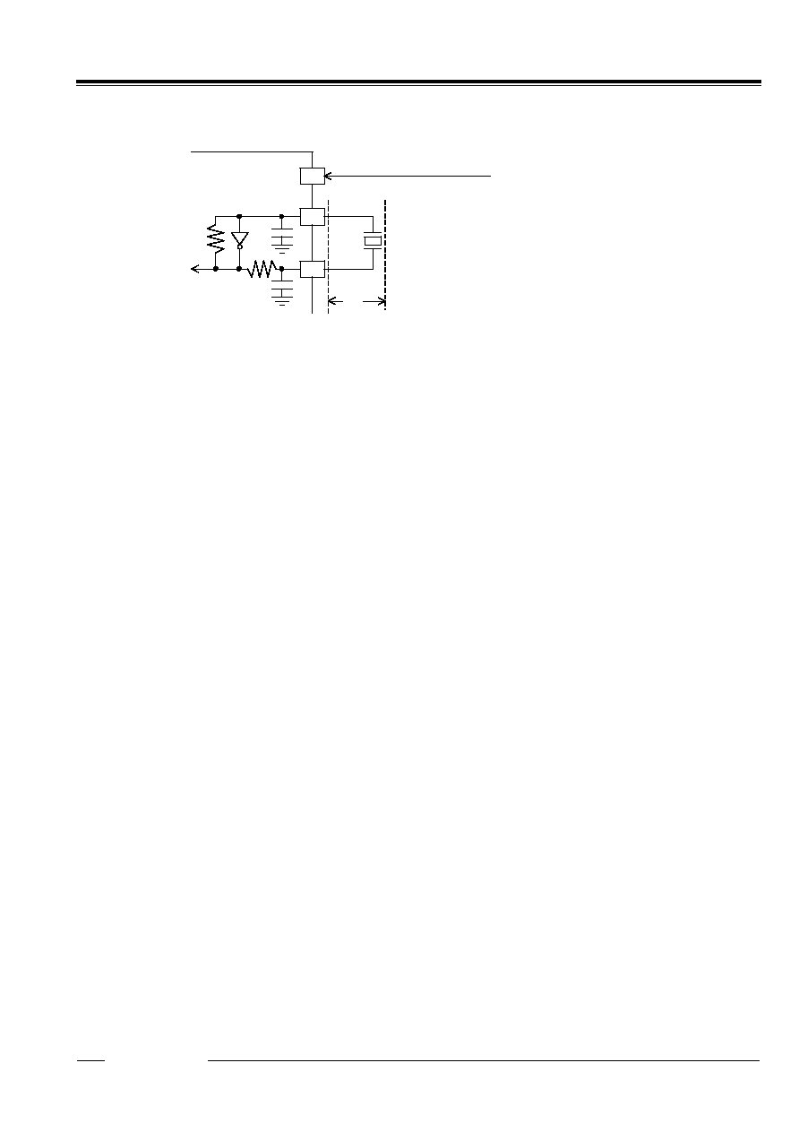
2-wires, SCL and SDA pins that are connected to I2C-Bus are used for transmit clock pulses and data
respectively. All ICs that are connected to these lines are designed that will not be clamped when a voltage
beyond supply voltage is applied to input or output pins. Open drain pins are used for output. This
construction allows communication of signals between ICs with different supply voltages by adding a pull-up
resistor to each signal line as shown in the figure below. Each IC is designed not to affect SCL and SDA
signal lines when power to each of these is turned off separately.
Micro-
Controller
RV5C386A
Other
Peripheral
Device
VDD1
VDD2
VDD3
VDD4
SCL
SDA
* For data interface, the following conditions
must be met:
VDD4
VDD1
VDD4
VDD2
VDD4
VDD3
* When the master is one, the micro-
controller is ready for driving SCL to "H" and
Rp of SCL may not be required.
Rp
Rp
Cautions on determining Rp resistance,
(1) Dropping voltage at Rp due to sum of input current or output current at off conditions on each IC pin
connected to the I
2
C-Bus shall be adequately small.
(2) Rising time of each signal be kept short even when all capacity of the bus is driven.
(3) Current consumed in I
2
C-Bus is small compared to the consumption current permitted for the entire
system.
When all ICs connected to I
2
C-Bus are CMOS type, condition (1) may usually be ignored since input current
and off-state output current is extremely small for the many CMOS type ICs. Thus the maximum resistance
of Rp may be determined based on (2), while the minimum on (3) in most cases.
In actual cases a resistor may be place between the bus and input/output pins of each IC to improve noise
margins in which case the Rp minimum value may be determined by the resistance.
Consumption current in the bus to review (3) above may be expressed by the formula below:
Bus consumption current
(Sum of input current and off state output current of all devices in standby mode )
◊
Bus standby duration
Bus stand-by duration + the Bus operation duration
+ Supply voltage
◊
Bus operation duration
◊
2
Rp resistance
◊
2
◊
(Bus stand-by duration + bus operation duration)
+ Supply voltage
◊
Bus capacity
◊
Charging/Discharging times per unit time
Operation of "
◊
2" in the second member denominator in the above formula is derived from assumption that
"L" duration of SDA and SCL pins are the half of bus operation duration. "
◊
2" in the numerator of the same
member is because there are two pins of SDA and SCL. The third member, (charging/discharging times per
unit time) means number of transition from "H" to "L" of the signal line.
PRELIMINARY RV5C386A
12345
- 19 -
Calculation example is shown below:
Pull-up resistor (Rp) = 10k
, Bus capacity = 50pF(both for SCL, SDA), Vdd=3v,
In a system with sum of input current and off-state output current of each pin = 0.1
µ
A,
I
2
C-Bus is used for 10ms every second while the rest of 990ms in the stand-by mode,
In this mode, number of transitions of the SCL pin from "H" to "L" state is 100 while SDA 50, every second.
Bus consumption current
0.1
µ
A
◊
990msec
990msec + 10msec
+ 3V
◊
10msec
◊
2
10K
◊
2
◊
(990msec + 10msec)
+ 3V
◊
50pF
◊
(100 + 50)
0.099
µ
A + 3.0
µ
A + 0.0225
µ
A
3.12
µ
A
Generally, the second member of the above formula is larger enough than the first and the third members,
bus consumption current may be determined by the second member is many cases.
14.1.2. Transmission System of I
2
C-Bus
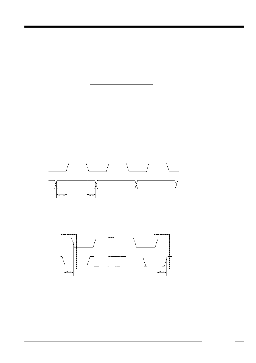
(1) Start Condition and Stop Condition
In I
2
C-Bus, SDA must be kept at a certain state while SCL is at the "H" state during data transmission as
shown below.
SCL
SDA
tSU;DAT
tHD;DAT
The SCL and SDA pins are at the "H" level when no data transmission is made. Changing the SDA from "H" to
"L" when the SCL and the SDA are "H" activates the Start Condition and access is started. Changing the SDA
from "L" to "H" when the SCL is "H" activates Stop Condition and accessing stopped. Generation of Start and
Stop Conditions are always made by the master (see the figure below).
SCL
SDA
tHD;STA
tSU;STO
Start Condition
Stop Condition
(2) Data transmission and its acknowledge
After Start condition is entered, data is transmitted by 1byte (8bits). Any bytes of data may be serially
transmitted. The receiving side will send an acknowledge signal to the transmission side each time 8bit data
is transmitted. The acknowledge signal is sent immediately after falling to "L" of SCL 8bit clock pulses of
data is transmitted, by releasing the SDA by the transmission side that has asserted the bus at that time and
by turning SDA to "L" by receiving side. When transmission of 1byte data next to preceding 1byte of data is
received the receiving side releases the SDA pin at falling edge of the SCL 9bit of clock pulses or when the
receiving side switches to the transmission side it starts data transmission. When the master is receiving
side, it generates no acknowledge signal after last 1byte of data from the slave to tell the transmitter that data
RV5C386A PRELIMINARY
12345
- 20 -
transmission has completed. The slave side (transmission side) continues to release the SDA pin so that
the master will be able to generate Stop Condition, after falling edge of the SCL 9bit of clock pulses.
SCL
from the master
SDA from
the transmission side
SDA from
the receiving side
1
2
8
9
Acknowledge
signal
Start
Condition
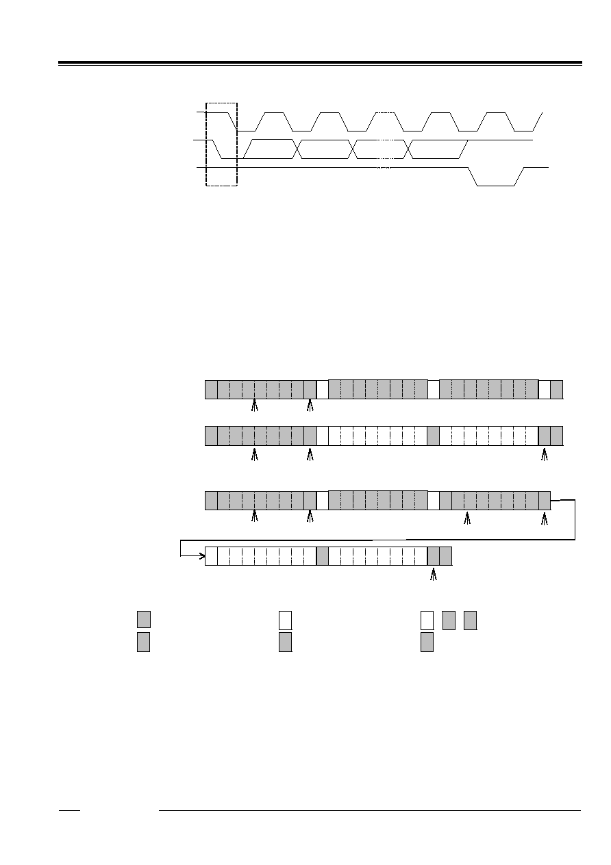
(3) Data Transmission Format in I
2
C-Bus
I
2
C-Bus has no chip enable signal line. In place of it, each device has a 7bit Slave Address allocated. The
first 1byte is allocated to this 7bit address and to the command (R/W) for which data transmission direction is
designated by the data transmission thereafter. 7bit address is sequentially transmitted from the MSB and 2
and after bytes are read, when 8bit is "H" and when write "L".
The Slave Address of the RV5C386A is specified at (0110010).
At the end of data transmission / receiving, Stop Condition is generated to complete transmission. However,
if start condition is generated without generating Stop Condition, Repeated Start Condition is met and
transmission / receiving data may be continue by setting the Slave Address again. Use this procedure when
the transmission direction needs to be change during one transmission.
S
A
A
Data
/A P
Data is written to the slave
from the master
S
0
A
Slave Address
Data
A
A P
When data is read from the
slave immediately after 7bit
addressing from the master
Master to slave
Slave to master
Sr
Repeated Start Condition
P
Stop Condition
A
A
/A Acknowledge Signal
R/W=1(Read)
(0110010)
Inform read has been completed by not generate
an acknowledge signal to the slave side.
Data
R/W=0(Write)
(0110010)
When the transmission
direction is to be changed
during transmission.
Sr
1
0
A
A
R/W=0(Write)
A
Data
R/W=1(Read)
(0110010)
S
1
A
/A P
Inform read has been completed by not generate
an acknowledge signal to the slave side.
Data
S
Start Condition
(0110010)
Slave Address
Salve Address
Slave Address
Data
Data
PRELIMINARY RV5C386A
12345
- 21 -
14.1.3.
Data Transmission Write Format in the RV5C386A
Although the I
2
C-Bus standard defines a transmission format for the slave allocated for each IC, transmission
method of address information in IC is not defined. The RV5C386A transmits data the internal address
pointer (4bit) and the Transmission Format Register (4bit) at the 1byte next to one which transmitted a Slave
Address and a write command. For write operation only one transmission format is available and (0000) is
set to the Transmission Format Register. The 3byte transmits data to the address specified by the internal
address pointer written to the 2byte. Internal address pointer setting are automatically incremented for
4byte and after. Note that when the internal address pointer is Fh, it will change to 0h on transmitting the
next byte.
1
A
S
0
A
Data
A
Data
A P
Example of data writing (When writing to internal address Eh to Fh)
Master to slave
Slave to master
S
Start Condition
P
Stop Condition
A
A
/A
Acknowledge signal
Address
Pointer
Eh
R/W=0(Write)
Slave Address
(0110010)
1
1
0
0
0
0
0
0 0 0
0
1 1
1
Transmission
Format
Register
0h
Writing of data to the
internal address Fh
Writing of data to the
internal address Eh
RV5C386A PRELIMINARY
12345
- 22 -
14.1.4.
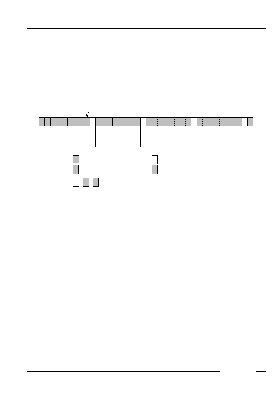
Data transmission read format of the RV5C386A
The RV5C386A allows the following three readout method of data an internal register.
1) The first method to reading data from the internal register is to specify an internal address by setting the
internal address pointer and the transmission format register described 14.1.3, generate the Repeated
Start Condition (See section 14.1.2-(3)) to change the data transmission direction to perform reading.
The internal address pointer is set to Fh when the Stop Condition is met. Therefore, this method of
reading allows no insertion of Stop Condition before the Repeated Start Condition. Set 0h to the
Transmission Format Register when this method used.
1
S
0
A
A
Data
/A P
Example 1 of Data Read (when data is read from 2h to 4h)
Master to slave
Slave to master
S
Start Condition
Sr
Repeated Start
Condition
A
A
/A
Acknowledge signal
Address
Pointer
2h
Repeated Start Condition
0
1
0
0
0
1
1
0 0 0
0
0
0
1
Transmission
Format
Register
0h
Sr
1
0
A
Slave Address
(0110010)
1
0
0 0
0
1
A
Data
A
Data
Reading of data from
the internal address 3h
R/W=1(Read)
R/W=0(Write)
P
Stop Condition
Slave Address
(0110010)
Reading of data from
the internal address 4h
Reading of data from
the internal address 2h
PRELIMINARY RV5C386A
12345
- 23 -
2) The second method to reading data from the internal register is to start reading immediately after writing
to the Internal Address Pointer and the Transmission Format Register. Although this method is not based
on I
2
C-Bus standard in a strict sense it still effective to shorten read time to ease load to the master. Set
4h to the transmission format register when this method used.
1
S
A
A
Data
/A P
Example 2 of data read (when data is read from internal addresses Eh to 1h)
Master to slave
Slave to Master
S
Start Condition
A
A
/A
Acknowledge Signal
Address
Pointer
Eh
0 1
1
0 0
0
1
Transmission
Format
Register
4h
1
0
A
Slave Address
(0110010)
1
0
0 0
0
1
A
Data
A
Data
Reading of data from
the internal address Eh
R/W=0(Write)
P
Stop Condition
Data
Reading of data from
the internal address Fh
Reading of data from
the internal address 0h
Reading of data from
the internal address 1h
RV5C386A PRELIMINARY
12345
- 24 -
3) The third method to reading data from the internal register is to start reading immediately after writing to
the Slave Address and R/W bit. Since the Internal Address Pointer is set to Fh by default as described
in 1), this method is only effective when reading is started from the Internal Address Fh.
S
A
A
Data
/A P
Example 3 of data read (when data is read from internal addresses Fh to 3h)
Master to slave
Slave to master
S
Start Condition
A
A
/A
Acknowledge Signal
1
0
A
Slave Address
(0110010)
1
0
0 1
0
1
A
Data
A
Data
R/W=1(Read)
P
Stop Condition
Data
Data
Reading of data from
the Internal Address Fh
Reading of data from
the Internal Address 0h
Reading of data from
the Internal Address 1h
Reading of data from
the Internal Address 2h
Reading of data from
the Internal Address 3h

PRELIMINARY RV5C386A
12345
- 25 -
14.1.5. Data Transmission under Special Condition
The RV5C386A holds the clock tentatively for duration from Start Condition to avoid invalid read or write
clock on carrying clock. When clock carried during this period, which will be adjusted within approx. 61
µ
s
from Stop Condition. To prevent invalid read or write, clock shall be made during one transmission
operation (from Start Condition to Stop Condition). When 0.5 to 1.0 second elapses after Start Condition,
any access to the RV5C386A is automatically released to release tentative hold of the clock, and access from
the CPU is forced to be terminated (The same action as made Stop Condition is received: automatic resume
function from I
2
C-Bus interface). Therefore, one access must be complete within 0.5 seconds. The
automatic resume function prevents delay in clock even if SCL is stopped from sudden failure of the system
during clock read operation.
Also a second Start Condition after the first Start Condition and before the Stop Condition is regarded
"Repeated Start Condition". Therefore, when 0.5 to 1.0 seconds passed after the first Start Condition, an
access to the RV5C386A is automatically released.
If access is tried after automatic resume function is activated, no acknowledge signal will be output for writing
while FFh will be output for reading.
The user shall always be able to access the real-time clock as long as three conditions are met.
(1) No Stop Condition shall be generated until clock read/write is started and completed.
(2) One cycle read/write operation shall be complete within 0.5 seconds.
(3) Do not make Start Condition within 61
µ
s from Stop Condition. When clock is carried during the access,
which will be adjusted within approx. 61
µ
s from Stop Condition.
Bad example of reading from seconds to hours (invalid read)
(Start Condition)
(Read of seconds)
(read of minutes)
(Stop Condition)
(Start Condition)
(Read
of hour)
(Stop Condition)
Assuming read was started at 05:59:59 P.M. and while reading seconds and minutes the time advanced to
06:00:00 P.M. At this time second digit is hold so read the read as 05:59:59. Then the RV5C386A confirms
(Stop Condition) and carries second digit being hold and the time change to 06:00:00 P.M. Then, when the
hour digit is read, it changes to 6. The wrong results of 06:59:59 will be read.
RV5C386A PRELIMINARY
12345
- 26 -
14.2.
Configuration of Oscillation Circuit and Correction of Time Count Deviations
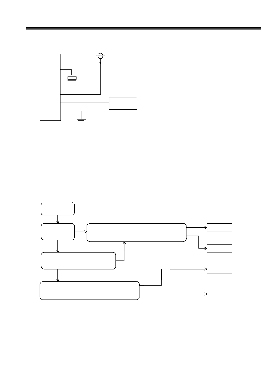
14.2.1. Configuration of Oscillation Circuit
OSCIN
OSCOUT
VDD
VDD
32kHz
RD
RF
CG
CD
A
The oscillation circuit is driven at a constant voltage of approximately 1.2 volts relative to the level of the VSS
pin input. As such, it is configured to generate an oscillating waveform with a peak-to-peak voltage on the
order of 1.2 volts on the positive side of the VSS pin input.
< Considerations in Handling Crystal Oscillators >
Generally, crystal oscillators have basic characteristics including an equivalent series resistance (R1)
indicating the ease of their oscillation and a load capacitance (CL) indicating the degree of their center
frequency. Particularly, crystal oscillators intended for use in the RV5C386A are recommended to have a
typical R1 value of 30k
and a typical CL value of 6 to 8pF. To confirm these recommended values,
contact the manufacturers of crystal oscillators intended for use in these particular models.
< Considerations in Installing Components around the Oscillation Circuit >
1) Install the crystal oscillator in the closest possible vicinity to the real-time clock ICs.
2) Avoid laying any signal lines or power lines in the vicinity of the oscillation circuit (particularly in the area
marked "A" in the above figure).
3) Apply the highest possible insulation resistance between the OSCIN and OSCOUT pins and the printed
circuit board.
4) Avoid using any long parallel lines to wire the OSCIN and OSCOUT pins.
5) Take extreme care not to cause condensation, which leads to various problems such as oscillation halt.
< Other Relevant Considerations >
1) For external input of 32.768-kHz clock pulses to the OSCIN pin:
DC coupling: Prohibited due to an input level mismatch.
AC coupling: Permissible except that the oscillation halt sensing circuit does not guarantee perfect
operation because it may cause sensing errors due to such factors as noise.
2) To maintain stable characteristics of the crystal oscillator, avoid driving any other IC through 32.768-kHz
clock pulses output from the OSCOUT pin.
Typical externally-equipped element
X'tal : 32.768kHz
(R1=30k
typ)
(CL=6pF to 8pF)
Standard values of internal elements
RF 15M
typ
RD 120k
typ
CG,CD 12pF typ
PRELIMINARY RV5C386A
12345
- 27 -
14.2.2. Measurement of Oscillation Frequency
Frequency
Counter
OSCIN
OSCOUT
32KOUT
VSS
32768Hz
VDD
CLKC
* 1) The RV5C386A is configured to generate 32.768-kHz clock pulses for output from the 32KOUT pin.
* 2) A frequency counter with 6 (more preferably 7) or more digits on the order of 1ppm is recommended for
use in the measurement of the oscillation frequency of the oscillation circuit.
* 3) The CLKC pin should be connected to the VDD pin as a pull-up resistor.
14.2.3. Adjustment of Oscillation frequency
The oscillation frequency of the oscillation circuit can be adjusted by varying procedures depending on the
usage of Model RV5C386A in the system into which they are to be built and on the allowable degree of time
count errors. The flow chart below serves as a guide to selecting an optimum oscillation frequency
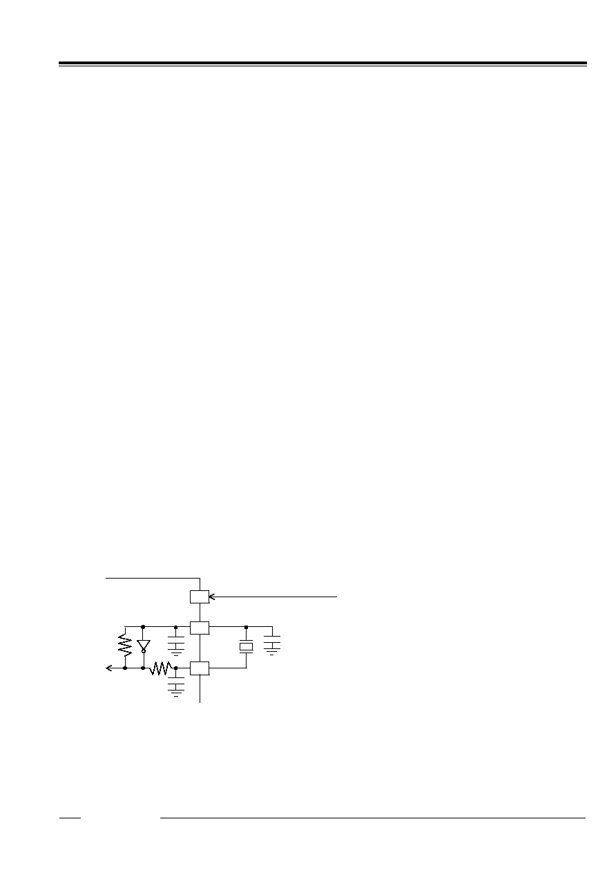
adjustment procedure for the relevant system.
Start
Course (B)
Use 32-kHz clock output without regard
to its frequency precision
NO
YES
Use 32-kHz
clock output?
YES
NO
Course (C)
Course (A)
Course (D)
YES
YES
NO
NO
Allowable time count precision on order of oscillation
frequency variations of crystal oscillator (*1) plus
frequency variations of RTC (*2)? (*3)
Allowable time count precision on order of oscillation
frequency variations of crystal oscillator (*1) plus
frequency variations of RTC (*2)? (*3)
* 1) Generally, crystal oscillators for commercial use are classified in terms of their center frequency depending
on their load capacitance (CL) and further divided into ranks on the order of
±
10,
±
20, and
±
50ppm
depending on the degree of their oscillation frequency variations.
* 2) Basically, Model RV5C386A is configured to cause frequency variations on the order of
±
5 to
±
10ppm at
normal temperature.
* 3) Time count precision as referred to in the above flow chart is applicable to normal temperature and actually
affected by the temperature characteristics and other properties of crystal oscillators.
RV5C386A PRELIMINARY
12345
- 28 -
Course (A)
When the time count precision of each RTC is not to be adjusted, the crystal oscillator intended for use in that
RTC may have any CL value requiring no presetting. The crystal oscillator may be subject to frequency
variations which are selectable within the allowable range of time count precision. Several crystal oscillators
and RTCs should be used to find the center frequency of the crystal oscillators by the method described in
"14.2. 2. Measurement of Oscillation Frequency" and then calculate an appropriate oscillation adjustment
value by the method described in "14.2. 4. Oscillation Adjustment Circuit" for writing this value to the
RV5C386A.
Course (B)
When the time count precision of each RTC is to be adjusted within the oscillation frequency variations of the
crystal oscillator plus the frequency variations of the real-time clock ICs, it becomes necessary to correct
deviations in the time count of each RTC by the method described in "14.2.4. Oscillation Adjustment
Circuit". Such oscillation adjustment provides crystal oscillators with a wider range of allowable settings of
their oscillation frequency variations and their CL values. The real-time clock IC and the crystal oscillator
intended for use in that real-time clock IC should be used to find the center frequency of the crystal oscillator
by the method described in "14.2.2. Measurement of Oscillation Frequency" and then confirm the center
frequency thus found to fall within the range adjustable by the oscillation adjustment circuit before adjusting
the oscillation frequency of the oscillation circuit. At normal temperature, the oscillation frequency of the
oscillator circuit can be adjusted by up to approximately
±
1.5ppm.
Course (C)
Course (C) together with Course (D) requires adjusting the time count precision of each RTC as well as the
frequency of 32.768-kHz clock pulses output from the 32KOUT pin. Normally, the oscillation frequency of
the crystal oscillator intended for use in the RTCs should be adjusted by adjusting the oscillation stabilizing
capacitors CG and CD connected to both ends of the crystal oscillator. The RV5C386A, which incorporate
the CG and the CD, require adjusting the oscillation frequency of the crystal oscillator through its CL value.
Generally, the relationship between the CL value and the CG and CD values can be represented by the
following equation:
CL = (CG
◊
CD)/(CG + CD) + CS where "CS" represents the floating capacity of the printed circuit board.
The crystal oscillator intended for use in the RV5C386A is recommended to have the CL value on the order of
6 to 8pF. Its oscillation frequency should be measured by the method described in "14.2.2. Measurement
of Oscillation Frequency". Any crystal oscillator found to have an excessively high or low oscillation
frequency (causing a time count gain or loss, respectively) should be replaced with another one having a
smaller and greater CL value, respectively until another one having an optimum CL value is selected. In
this case, the bit settings disabling the oscillation adjustment circuit (see "14.2.4. Oscillation Adjustment
Circuit") should be written to the oscillation adjustment register.
Incidentally, the high oscillation frequency of the crystal oscillator can also be adjusted by adding an external
oscillation stabilization capacitor CGOUT as illustrated in the diagram below.
OSCIN
OSCOUT
VDD
VDD
32kHz
RD
RF
*1)
CD
CG
CGout
Course (D)
It is necessary to select the crystal oscillator in the same manner as in Course (C) as well as correct errors in
the time count of each RTC in the same manner as in Course (B) by the method described in "14.2.4.
Oscillation Adjustment Circuit".
*1) The CGOUT should have a capacitance ranging
from 0 to 15 pF.

PRELIMINARY RV5C386A
12345
- 29 -
14.2.4. Oscillation Adjustment Circuit
The oscillation adjustment circuit can be used to correct a time count gain or loss with high precision by
varying the number of 1-second clock pulses once per 20 seconds. When such oscillation adjustment is not
to be made, the oscillation adjustment circuit can be disabled by writing the settings of "*, 0, 0, 0, 0, 0, *" ("*"
representing "0" or "1") to the F6, F5, F4, F3, F2, F1, and F0 bits in the oscillation adjustment circuit.
Conversely, when such oscillation adjustment is to be made, an appropriate oscillation adjustment value can
be calculated by the equation below for writing to the oscillation adjustment circuit.
(1) When Oscillation Frequency (* 1) Is Higher Than Target Frequency (* 2) (Causing Time Count Gain)
Oscillation adjustment value (*3) = (Oscillation frequency - Target Frequency + 0.1)
Oscillation frequency
◊
3.051
◊
10
-6
(Oscillation Frequency ≠ Target Frequency)
◊
10 + 1
* 1) Oscillation frequency:
Frequency of clock pulse output from the 32KOUT pin at normal temperature in the manner described in
"14.2.2. Measurement of Oscillation Frequency".
* 2) Target frequency:
Desired frequency to be set. Generally, a 32.768-kHz crystal oscillator has such temperature
characteristics as to have the highest oscillation frequency at normal temperature. Consequently, the
crystal oscillator is recommended to have target frequency settings on the order of 32.768 to 32.76810 kHz
(+3.05ppm relative to 32.768 kHz). Note that the target frequency differs depending on the environment or
location where the equipment incorporating the RTC is expected to be operated.
* 3) Oscillation adjustment value:
Value that is to be finally written to the F0 to F6 bits in the Oscillation Adjustment Register and is represented
in 7-bit coded decimal notation.
(2) When Oscillation Frequency Is Equal To Target Frequency (Causing Time Count neither Gain nor Loss)
Oscillation adjustment value = 0, +1, -64, or ≠63
(3) When Oscillation Frequency Is Lower Than Target Frequency (Causing Time Count Loss)
Oscillation adjustment value = (Oscillation frequency - Target Frequency)
Oscillation frequency
◊
3.051
◊
10
-6
(Oscillation Frequency ≠ Target Frequency)
◊
10
Oscillation adjustment value calculations are exemplified below
(A) For an oscillation frequency = 32768.85Hz and a target frequency = 32768.05Hz
Oscillation adjustment value = (32768.85 - 32768.05 + 0.1) / (32768.85
◊
3.051
◊
10
-6
)
(32768.85 - 32768.05)
◊
10 + 1
= 9.001
9
In this instance, write the settings (F6,F5,F4,F3,F2,F1,F0)=(0,0,0,1,0,0,1) in the oscillation adjustment
register. Thus, an appropriate oscillation adjustment value in the presence of any time count gain
represents a distance from 01h.
(B) For an oscillation frequency = 32763.95Hz and a target frequency = 32768.05Hz
Oscillation adjustment value = (32763.95 - 32768.05) / (32763.95
◊
3.051
◊
10
-6
)
(32763.95 - 32768.05)
◊
10
= -41.015
-41
To represent an oscillation adjustment value of - 41 in 7-bit coded decimal notation, subtract 41 (29h)
from 128 (80h) to obtain 57h. In this instance, write the settings of (F6,F5,F4,F3,F2,F1,F0) =
(1,0,1,0,1,1,1) in the oscillation adjustment register. Thus, an appropriate oscillation adjustment value
in the presence of any time count loss represents a distance from 80h.
Oscillation adjustment involves an adjustment differential of approximately
±
1.5ppm from the target
frequency at normal temperature.
RV5C386A PRELIMINARY
12345
- 30 -
Notes:
1) Oscillation adjustment does not affect the frequency of 32.768-kHz clock pulses output from the 32KOUT pin.
2) Oscillation adjustment value range: When the oscillation frequency is higher than the target frequency
(causing a time count gain), an appropriate time count gain ranges from -3.05ppm to -189.2ppm with the
settings of "0, 0, 0, 0, 0, 1, 0" to "0, 1, 1, 1, 1, 1, 1" written to the F6, F5, F4, F3, F2, F1, and F0 bits in the
oscillation adjustment register, thus allowing correction of a time count gain of up to +189.2ppm. Conversely,
when the oscillation frequency is lower than the target frequency (causing a time count loss), an appropriate
time count gain ranges from +3.05ppm to +189.2ppm with the settings of "1, 1, 1, 1, 1, 1, 1" to "1, 0, 0, 0, 0, 1,
0" written to the F6, F5, F4, F3, F2, F1, and F0 bits in the oscillation adjustment register, thus allowing
correction of a time count loss of up to -189.2ppm.
14.3.
Oscillation Halt Sensing and Supply Voltage Monitoring
The oscillation halt sensing circuit is configured to record a halt on oscillation by 32.768-kHz clock pulses.
The supply voltage monitoring circuit is configured to record a drop in supply voltage below a threshold
voltage of 2.1 or 1.6v. Both the flag bits of these circuits (i.e. the XSTP bit for the former and the VDET bit
for the latter) in the control register 2, are maintained "1" until they are reset by the setting of 0 in the same
bits.
When the XSTP bit is set to 1 for the oscillation halt sensing circuit, the VDET bit is reset to 0 for the supply
voltage monitoring circuit. The relationship between the XSTP and VDET bits is shown in the table below.
XSTP
VDET
Conditions of supply voltage and oscillation
0
0
No drop in supply voltage below threshold voltage and no halt in oscillation
0
1
Drop in supply voltage below threshold voltage and no halt in oscillation
1
*
Halt on oscillation
32768Hz Oscillation
Supply voltage monitoring
(VDET)
Oscillation halt sensing
(XSTP)
Threshold voltage (2.1V or 1.6V)
Normal voltage detector
VDET
0
Supply voltage
XSTP,VDET
0
Internal initiali-
zation period
(1 to 2 sec.)
XSTP,VDET
0
When the XSTP bit is set to 1 in the control register 2, the F6 to F0, WALE, DALE, /12
24, SCRATCH3, TEST,
CT2, CT1, CT0, VDSL, VDET, SCRATCH1, SCRATCH2, CTFG, WAFG, and DAFG bits are reset to 0 in the
oscillation adjustment register, the control register 1, and the control register 2. The XSTP bit is also set to 1
at power-on from 0 volts. Note that the XSTP bit may be locked upon instantaneous power-down.
PRELIMINARY RV5C386A
12345
- 31 -
< Considerations in Using Oscillation Halt Sensing Circuit >
Be sure to prevent the oscillation halt sensing circuit from malfunctioning by preventing the following:
1) Instantaneous power-down on the VDD
2) Condensation on the crystal oscillator
3) On-board noise to the crystal oscillator
4) Applying to individual pins voltage exceeding their respective maximum ratings
In particular, note that the XSTP bit may fail to be set to 1 in the presence of any applied supply voltage as
illustrated below in such events as backup battery installation. Further, give special considerations to prevent
excessive chattering in the oscillation halt sensing circuit.
VDD
< Supply Voltage Sensing Circuit >
The Supply voltage monitoring circuit is configured to conduct a sampling operation during an interval of 7.8ms per
second to check for a drop in supply voltage below a threshold voltage of 2.1 or 1.6v for the VDSL bit setting of 0 (the
default setting) or 1, respectively, in the Control Register 2, thus minimizing supply current requirements as illustrated in
the timing chart below. This circuit suspends a sampling operation once the VDET bit is set to 1 in the Control Register
2.
VDET
(D6 at Address Fh)
XSTP
VDD
Threshold voltage of 2.1 or 1.6v
1s
VDET
0
7.8ms
Sampling operation by supply
voltage monitoring circuit
Internal initiali-
zation period
(1 to 2 sec.)
XSTP, VDET
0
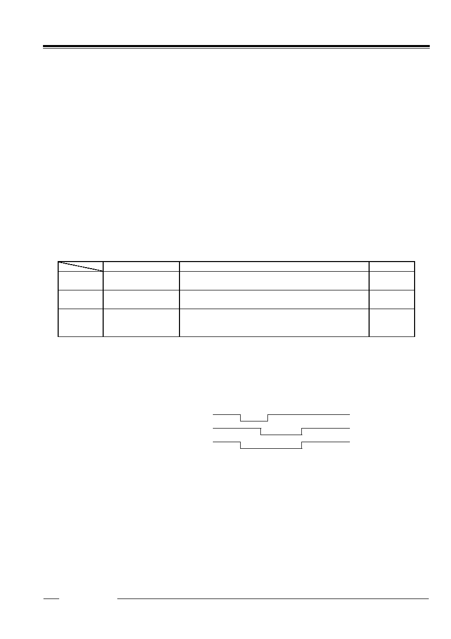
RV5C386A PRELIMINARY
12345
- 32 -
14.4.
Alarm and Periodic Interrupt
The RV5C386A incorporates the alarm interrupt circuit and the periodic interrupt circuit that are configured to
generate alarm signals and periodic interrupt signals, respectively, for output from the /INTRA or /INTRB pins
as described below.
(1) Alarm Interrupt Circuit
The alarm interrupt circuit is configured to generate alarm signals for output from the /INTRA or /INTRB,
which is driven low (enabled) upon the occurrence of a match between current time read by the time counters
(the day-of-week, hour, and minute counters) and alarm time preset by the alarm registers (the Alarm_W
registers intended for the day-of-week, hour, and minute digit settings and the Alarm_D registers intended for
the hour and minute digit settings). The Alarm_W is output from the /INTRB, and the Alarm_D is output
from /INTRA.
(2) Periodic Interrupt Circuit
The periodic interrupt circuit is configured to generate either clock pulses in the pulse mode or interrupt
signals in the level mode for output from the /INTRA pin depending on the CT2, CT1, and CT0 bit settings in
the control register 1.
The above two types of interrupt signals are monitored by the flag bits (i.e. the WAFG, DAFG, and CTFG bits
in the Control Register 2) and enabled or disabled by the enable bits (i.e. the WALE, DALE, CT2, CT1, and
CT0 bits in the Control Register 1) as listed in the table below.
Flag bits
Enable bits
Output Pin
Alarm_W
WAFG
(D1 at Address Fh)
WALE
(D7 at Address Eh)
/INTRB
Alarm_D
DAFG
(D0 at Address Fh)
DALE
(D6 at Address Eh)
/INTRA
Peridic
Interrupt
CTFG
(D2 at Address Fh)
CT2=CT1=CT0=0
(These bit setting of "0" disable the Periodic Interrupt)
(D2 to D0 at Address Eh)
/INTRA
* At power-on, when the WALE, DALE, CT2, CT1, and CT0 bits are set to 0 in the Control Register 1, the
/INTRA and /INTRB pins are driven high (disabled).
* When two types of interrupt signals are output simultaneously from the /INTRA pin, the output from the
/INTRA pin becomes an OR waveform of their negative logic.
Example: Combined Output to /INTRA Pin Under Control of
/ALARM_D and Periodic Interrupt
Periodic Interrupt
/INTRA
/Alarm_D
In this event, which type of interrupt signal is output from the /INTRA pin can be confirmed by reading the DAFG,
and CTFG bit settings in the Control Register 2.
14.4.1. Alarm Interrupt
The alarm interrupt circuit is controlled by the enable bits (i.e. the WALE and DALE bits in the Control
Register 1) and the flag bits (i.e. the WAFG and DAFG bits in the Control Register 2). The enable bits can
be used to enable this circuit when set to 1 and to disable it when set to 0. When intended for reading, the
flag bits can be used to monitor alarm interrupt signals. When intended for writing, the flag bits will cause no
event when set to 1 and will drive high (disable) the alarm interrupt circuit when set to 0.
The enable bits will not be affected even when the flag bits are set to 0. In this event, therefore, the alarm
interrupt circuit will continue to function until it is driven low (enabled) upon the next occurrence of a match
between current time and preset alarm time.
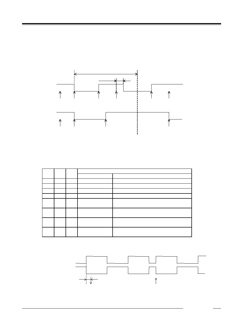
PRELIMINARY RV5C386A
12345
- 33 -
The alarm function can be set by presetting desired alarm time in the alarm registers (the Alarm_W Registers
for the day-of-week digit settings and both the Alarm_W Registers and the Alarm_D Registers for the hour
and minute digit settings) with the WALE and DALE bits once set to 0 and then to 1 in the Control Register 1.
Note that the WALE and DALE bits should be once set to 0 in order to disable the alarm interrupt circuit upon
the coincidental occurrence of a match between current time and preset alarm time in the process of setting
the alarm function.
current time =
preset alarm time
WALE
1
(DALE)
WALE
0
(DALE)
Interval (1min.) during which a match
between current time and preset alarm time
occurs
current time =
preset alarm time
WAFG
0
(DAFG)
Max.61.1
µ
s
/INTRB
(/INTRA)
WALE
1
(DALE)
WALE
1
(DALE)
current time =
preset alarm time
WALE
0
(DALE)
current time =
preset alarm time
/INTRB
(/INTRA)
14.4.2. Periodic Interrupt
Setting of the periodic selection bits (CT2 to CT0) enables periodic interrupt to the CPU. There are two
waveform modes: pulse mode and level mode. In the pulse mode, the output has a waveform duty cycle of
around 50%. In the level mode, the output is cyclically driven low and, when the CTFG bit is set to 0, the
output is return to High (OFF).
Description
CT2
CT1
CT0
Wave form mode
Interrupt Cycle and Falling Timing
0
0
0
-
OFF(H)
(Default)
0
0
1
-
Fixed at "L"
0
1
0
Pulse Mode *1)
2Hz(Duty50%)
0
1
1
Pulse Mode *1)
1Hz(Duty50%)
1
0
0
Level Mode *2)
Once per 1 second (Synchronized with
Second counter increment)
1
0
1
Level Mode *2)
Once per 1 minute (at 00 seconds of every
Minute)
1
1
0
Level Mode *2)
Once per hour (at 00 minutes and 00
Seconds of every hour)
1
1
1
Level Mode *2)
Once per month (at 00 hours, 00 minutes,
and 00 seconds of first day of every month)
*1) Pulse Mode: 2-Hz and 1-Hz clock pulses are output in synchronization with the increment of the second
counter as illustrated in the timing chart below.
/INTRA Pin
Rewriting of the second counter
CTFG Bit
Approx. 92
µ
s
(Increment of second counter)
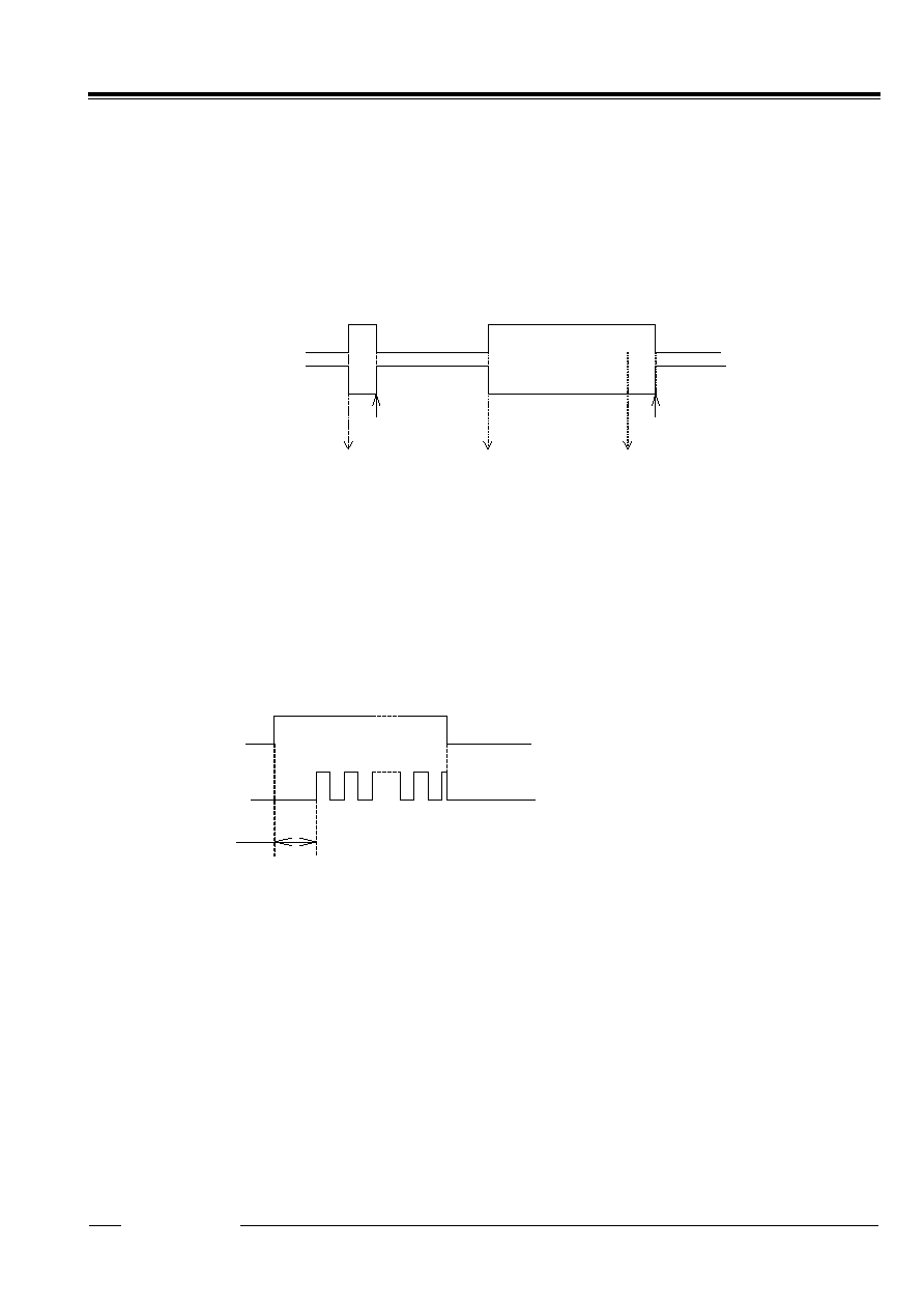
RV5C386A PRELIMINARY
12345
- 34 -
In the pulse mode, the increment of the second counter is delayed by approximately 92
µ
s from the falling edge of
clock pulses. Consequently, time readings immediately after the falling edge of clock pulses may appear to lag
behind the time counts of the real-time clocks by approximately 1 second. Rewriting the second counter will
reset the other time counters of less than 1 second, driving the /INTRA pin low.
*2) Level Mode: Periodic interrupt signals are output with selectable interrupt cycle settings of 1 second, 1
minute, 1 hour, and 1 month. The increment of the second counter is synchronized with the
falling edge of periodic interrupt signals. For example, periodic interrupt signals with an
interrupt cycle setting of 1 second are output in synchronization with the increment of the second
counter as illustrated in the timing chart below.
/INTRA Pin
(Increment of
second counter)
CTFG Bit
Setting CTFG bit to 0
Setting CTFG bit to 0
(Increment of
second counter)
(Increment of
second counter)
*1), *2) When the oscillation adjustment circuit is used, the interrupt cycle will fluctuate once per 20sec. as follows:
Pulse Mode: The "L" period of output pulses will increment or decrement by a maximum of
±
3.784ms. For
example, 1-Hz clock pulses will have a duty cycle of 50
±
0.3784%.
Level Mode: A periodic interrupt cycle of 1 second will increment or decrement by a maximum of
±
3.784 ms.
14.5.
32-kHz CLOCK OUTPUT
For the RV5C386A, 32.768-kHz clock pulses are output from the 32KOUT pin when the CLKC pin is set to
high. If CLKC is set to low or opened, the 32KOUT pin is driven low.
For the RV5C386A, the 32KOUT pin output is synchronized with CLKC pin input as illustrated in the timing
chart below.
32KOUT pin
CLKC pin
Max.76.3
µ
s
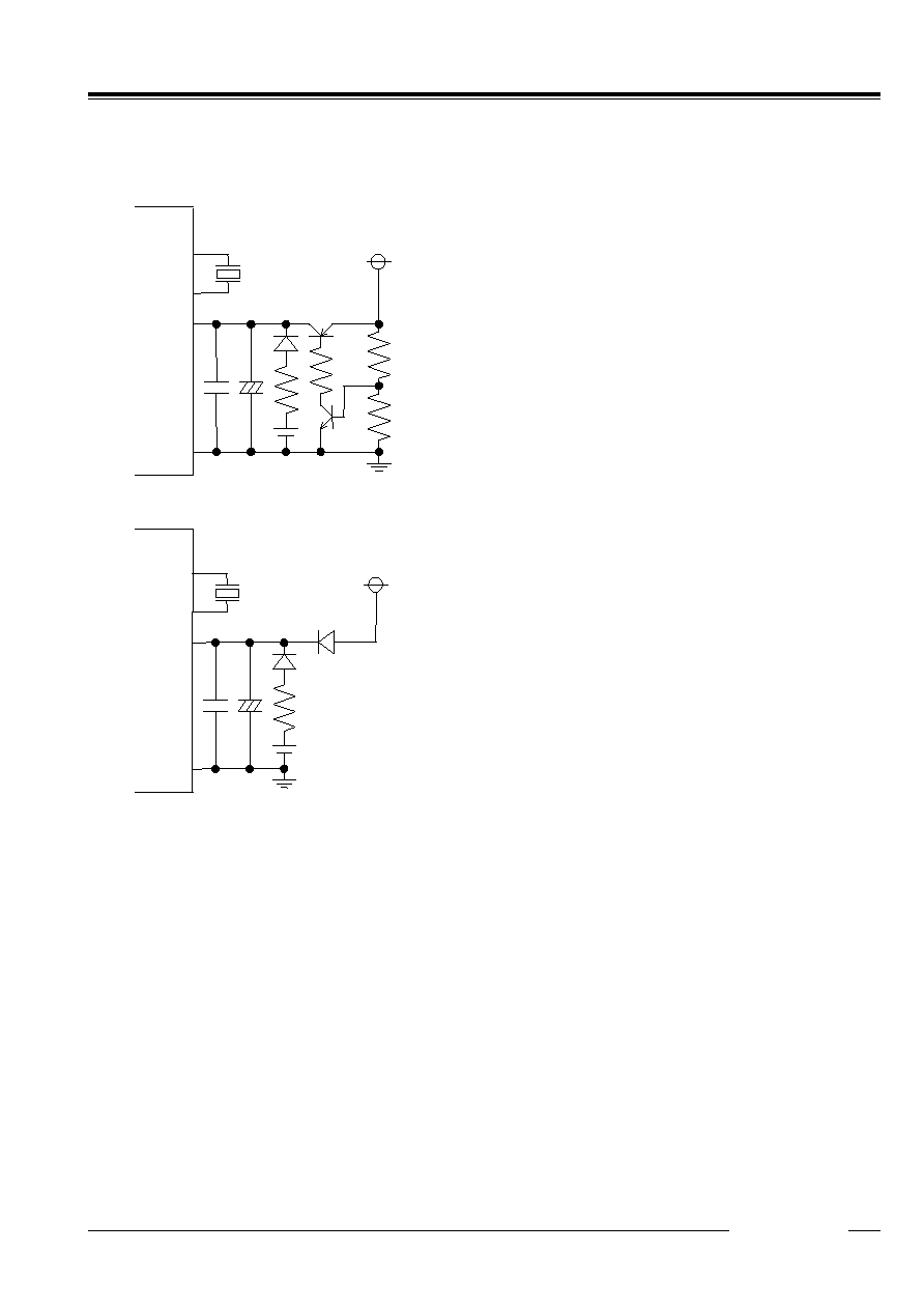
PRELIMINARY RV5C386A
12345
- 35 -
14.6.
Typical Applications
14.6.1. Typical Power Circuit Configurations
Sample circuit configuration 1
VDD
OSCIN
OSCOUT
VSS
32768Hz
System power supply
*1)
Sample circuit configuration 2
*1)
OSCIN
OSCOUT
VSS
32768Hz
System power supply
VDD
*1)
Install bypass capacitors for high-frequency
and low-frequency applications in parallel in
close vicinity to the RV5C386A.
*1) When using an OR diode as a power supply for
the RV5C386A ensure that voltage exceeding
the absolute maximum rating of VDD+0.3v is
not applied the 32KOUT pin.
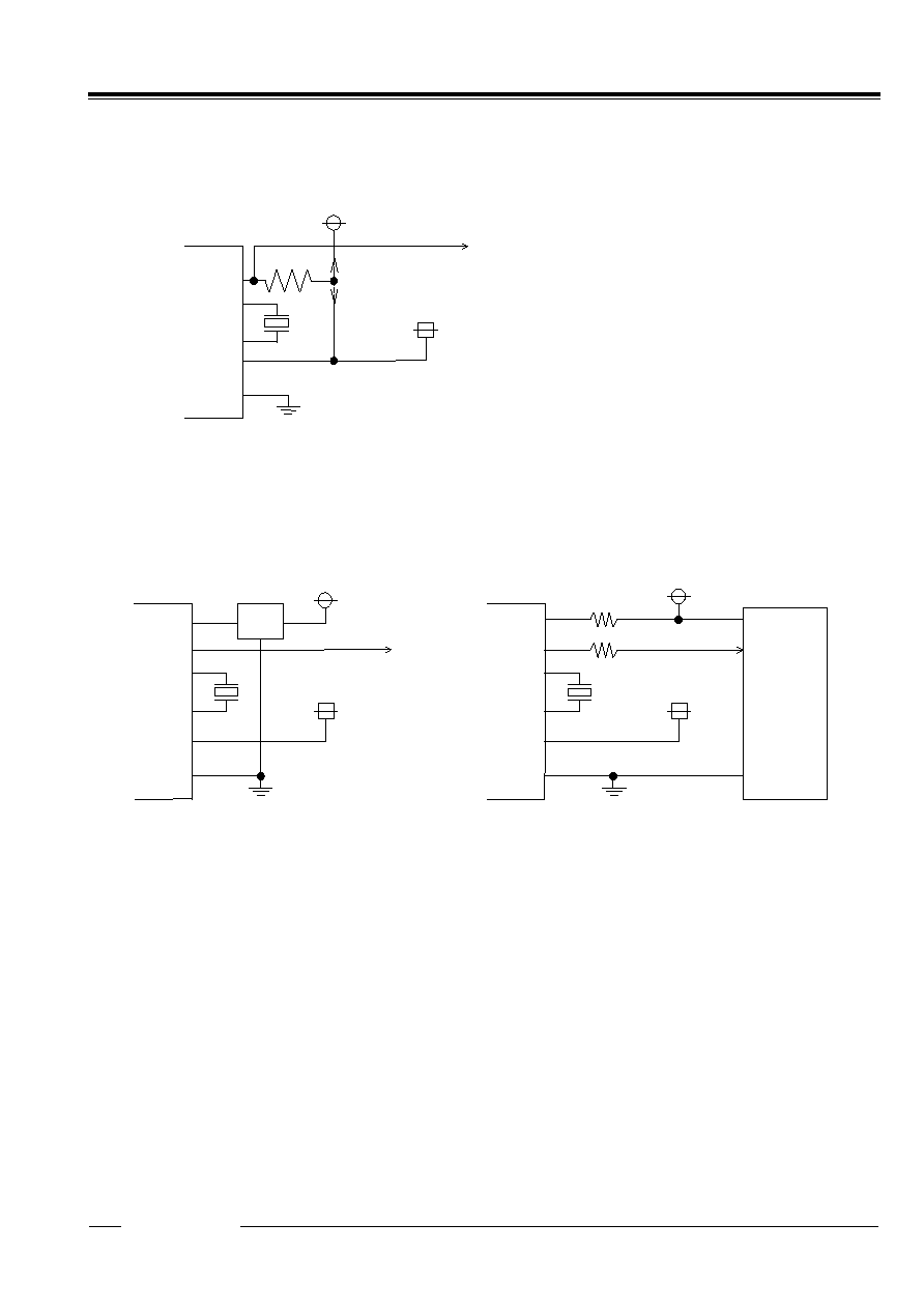
RV5C386A PRELIMINARY
12345
- 36 -
14.6.2. Connection of /INTRA and /INTRB Pin
The /INTRA and /INTRB pins follow the N-channel open drain output logic and contains no protective diode
on the power supply side. As such, it can be connected to a pull-up resistor of up to 5.5 volts regardless of
supply voltage.
VDD
OSCIN
OSCOUT
/INTRA or /INTRB
*1)
32768Hz
B
A
Backup power supply
System power supply
VSS
14.6.3. Connection of 32KOUT Pin
As the 32KOUT pin is CMOS output, the power supply voltage of the RV5C386A and any devices to be
connected to the 32KOUT should be same. When the devices is powered down, the 32KOUT output should
be disabled.
When the CLKC pin is connected to the system power supply through the pull-up resistor, the pull-up resistor
should be 0
to 10k
, and the 32KOUT pin should be connect to the host through the resistor (approx.
10k
).
VDD
OSCIN
OSCOUT
CLKC
VSS
32768Hz
System power supply
32KOUT
RN5VL
XXC
Back-up power supply
VDD
OSCIN
OSCOUT
Host
VSS
32768Hz
Back-up power supply
System power supply
Approx. 10K
32KOUT
0 to10K
CLKC
*1) Depending on whether the /INTRA and /INTRB
pins are to be used during battery backup, it should
be connected to a pull-up resistor at the following
different positions:
(1) Position A in the left diagram when it is not to be
used during battery backup.
(2) Position B in the left diagram when it is to be used
during battery backup.
PRELIMINARY RV5C386A
12345
- 37 -
14.7.
Typical Characteristics
Test Circuit
Frequency
Counter
VDD
OSCIN
OSCOUT
32KOUT
VSS
32768Hz
Timekeeping Current vs. Supply voltage Timekeeping Current vs. Supply voltage
(with no 32-kHz clock output) (with 32-kHz clock output)
(SCL,SDA="H", CLKC="L" Output=Open, Topt=25
∞
C) (SCL,SDA="H", CLKC="H" Output=Open,
Topt=25
∞
C)
0
0.2
0.4
0.6
0.8
1
0
1
2
3
4
5
6
Supply Voltage VDD(v)
Timekeeping Current IDD (uA)
0
0.5
1
1.5
2
2.5
3
0
1
2
3
4
5
6
Supply Voltage VDD(v)
Timekeeping Current IDD(uA)
CPU Access Current vs. SCL Clock Frequency Timekeeping Current vs. Operating Temperature
(Output=Open,Topt=25
∞
C) (with no 32-kHz clock output)
(SCL,SDA=Open, Output=Open, )
0
5
10
15
20
0
100
200
300
400
500
SCL Clock Frequency (kHz)
CPU Access Current IDD(uA)
0
0.5
1
1.5
2
-60 -40 -20
0
20 40
60 80 100
Operating Temperature Topt(
∞
C)
Timekeeping Current IDD(uA)
VDD=5v
VDD=3v
X'tal: 32.768kHz
(R1=30k
typ)
(CL=6pF to 8pF)
Topt: 25C
∞
Output: Open
RV5C386A PRELIMINARY
12345
- 38 -
Oscillation Frequency Deviation vs. External CG Oscillation Frequency Deviation vs. Supply Voltage
(VDD=3v,Topt=25
∞
C, (Topt=25
∞
C,VDD=3v as standard)
External CG=0pF as standard)
-40
-35
-30
-25
-20
-15
-10
-5
0
5
10
0
5
10
15
20
External CG (pF)
Oscillation Frequency Devitation
(ppm)
-5
-4
-3
-2
-1
0
1
2
3
4
5
0
1
2
3
4
5
6
Supply Voltage VDD(v)
Oscillation Frequency
Devitation (ppm)
Oscillation Frequency Deviation vs. Operating Temperature
Oscillation Start Time vs. Supply Voltage
(VDD=3v, Topt=25
∞
C standard) (Topt=25
∞
C)
-140
-120
-100
-80
-60
-40
-20
0
20
-60 -40 -20 0
20 40 60 80 10
0
Operating Temperature Topt(
∞
C)
Oscillation Frequency
Devitation (ppm)
0
100
200
300
400
500
0
1
2
3
4
5
6
Supply Voltage VDD(v)
Oscillation Start Time (ms)
VOL vs. IOL Input Current to CLKC pin vs. Supply Voltage
(SDA, /INTRA, /INTRB Pin) (Topt=25
∞
C)
(Topt=25
∞
C)
0
5
10
15
20
25
30
0
0.2
0.4
0.6
0.8
1
VOL (v)
IOL (mA)
0
0.2
0.4
0.6
0.8
1
0
1
2
3
4
5
6
Supply Voltage VDD(v)
ICLKC(uA)
VDD=5v
VDD=3v
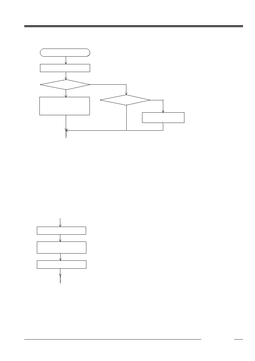
PRELIMINARY RV5C386A
12345
- 39 -
14.8.
Typical Software-based Operations
14.8.1. Initialization at Power-on
Start
*1)
Yes
No
VDET=0?
Warning Back-up
Battery Run-down
Set Oscillation Adjustment
Register and Control
Register 1 and 2, etc.
Power-on
*2)
*4)
*3)
XSTP=1?
Yes
No
*1) After power-on from 0 volt, the start of oscillation and the process of internal initialization require a time span
on the order of 1 to 2sec, so that access should be done after the lapse of this time span or more.
*2) The XSTP bit setting of 0 in the Control Register 1 indicates power-on from backup battery and not from 0v.
The XSTP bit may fail to be set to 1 in the presence of any excessive chattering in power supply in such
events as installing backup battery. Should there be any possibility of this failure occurring, it is
recommended to initialize Model RV5C386A RTCs regardless of the current XSTP bit setting. For further
details, see "14.3. Oscillation Halt Sensing and Supply Voltage Monitoring".
*3) This step is not required when the supply voltage monitoring circuit is not used.
*4) This step involves ordinary initialization including the Oscillation Adjustment Register and interrupt cycle
settings, etc.
14.8.2. Writing of Time and Calendar Data
Write to Time Counter and
Calendar Counter
*2)
Stop Condition
*3)
Start Condition
*1)
*1) When writing to clock and calendar counters, do not insert Stop Condition
until all times from second to year have been written to prevent error in
writing time. (Detailed in "14.1.5. Data Transmission under Special
Condition".
*2) Any writing to the second counter will reset divider units lower than the
second digits.
*3) Take care so that process from Start Condition to Stop Condition will be
complete within 0.5sec. (Detailed in "14.1.5. Data Transmission under
Special Condition".
The RV5C386A may also be initialized not at power-on but in the process
of writing time and calendar data.
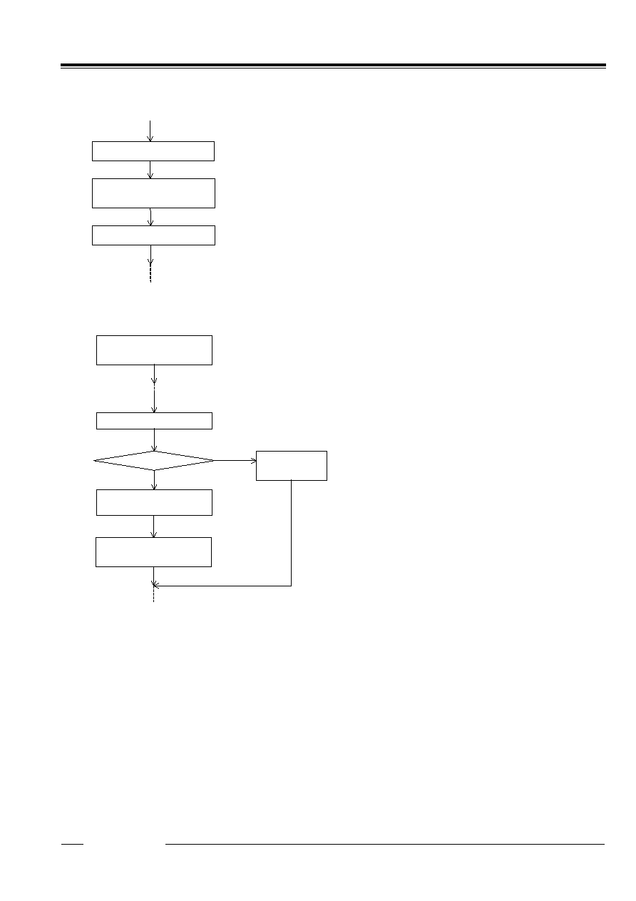
RV5C386A PRELIMINARY
12345
- 40 -
14.8.3. Reading Time and Calendar Data
(1) Ordinary Process of Reading Time and Calendar Data
Read from Time Counter
and Calendar Counter
*2)
Start Condition
Start Condition
*1)
(2) Basic Process of Reading Time and Calendar Data with Periodic Interrupt Function
*2)
Other Interrupt
Processes
Set Periodic Interrupt
Cycle Selection Bits
CTFG=1?
Read from Time Counter
and Calendar Counter
Yes
No
Control Register 2
(X1X1X011)
Generate Interrupt in CPU
*1)
*3)
*1) When writing to clock and calendar counters, do not insert Stop Condition
until all times from second to year have been written to prevent error in
writing time. (Detailed in "14.1.5. Data Transmission under Special
Condition".
*2) Take care so that process from Start Condition to Stop Condition will be
complete within 0.5sec. (Detailed in "14.1.5. Data Transmission under
Special Condition".
*1) This step is intended to select the level mode as a
waveform mode for the periodic interrupt function.
*2) This step must be completed within 0.5 second.
*3) This step is intended to set the CTFG bit to 0 in the
Control Register 2 to cancel an interrupt to the CPU.
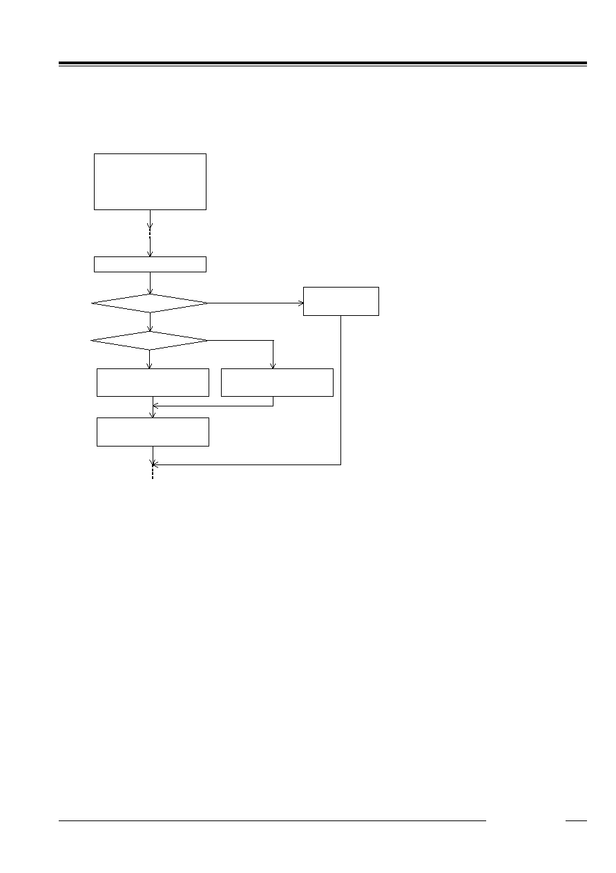
PRELIMINARY RV5C386A
12345
- 41 -
(3) Applied Process of Reading Time and Calendar Data with Periodic Interrupt Function
Time data need not be read from all the time counters when used for such ordinary purposes as time count indication. This
applied process can be used to read time and calendar data with substantial reductions in the load involved in such reading.
For Time Indication in "Day-of-Month, Day-of-week, Hour, Minute, and Second" Format:
*2)
Other interrupts
Processes
Control Register 1
(XXXX0100)
Control Register 2
(X1X1X011)
Sec.=00?
Yes
No
Use Previous Min.,Hr.,
Day,and Day-of-week data
Generate interrupt to CPU
*1)
*3)
CTFG=1?
Control Register 2
(X1X1X011)
Yes
Read Min.,Hr.,Day,
and Day-of-week
*4)
No
*1) This step is intended to select the level
mode as a waveform mode for the
periodic interrupt function.
*2) This step must be completed within 0.5
sec.
*3) This step is intended to read time data
from all the time counters only in the
first session of reading time data after
writing time data.
*4) This step is intended to set the CTFG
bit to 0 in the Control Register 2 to
cancel an interrupt to the CPU.

RV5C386A PRELIMINARY
12345
- 42 -
14.8.4. Interrupt Process
(1) Periodic Interrupt
*2)
Other Interrupt
Processes
Set Periodic Interrupt
Cycle Selection Bits
CTFG=1?
Conduct
Periodic Interrupt
Yes
No
Control Register 2
(X1X1X011)
Generate Interrupt to CPU
*1)
(2) Alarm Interrupt
*3)
Other Interrupt
Processes
Set Alarm Min., Hr., and
Fay-of-week Registers
WAFG or DAFG=1?
Conduct Alarm Interrupt
Yes
No
Control Register 2
(X1X1X101)
Generate Interrupt to CPU
*1)
WALE or DALE
1
WALE or DALE
0
*2)
*1) This step is intended to once disable the alarm
interrupt circuit by setting the WALE or DALE bits to 0
in anticipation of the coincidental occurrence of a
match between current time and preset alarm time in
the process of setting the alarm interrupt function.
*2) This step is intended to enable the alarm interrupt
function after completion of all alarm interrupt
settings.
*3) This step is intended to once cancel the alarm
interrupt function by writing the settings of "X,1,X,
1,X,1,0,1" and "X,1,X,1,X,1,1,0" to the Alarm_W
Registers and the Alarm_D Registers, respectively.
*1) This step is intended to select the level mode as a
waveform mode for the periodic interrupt function.
*2) This step is intended to set the CTFG bit to 0 in the
Control Register 2 to cancel an interrupt to the
CPU.