 | ÐлекÑÑоннÑй компоненÑ: BA6129AF | СкаÑаÑÑ:  PDF PDF  ZIP ZIP |
Äîêóìåíòàöèÿ è îïèñàíèÿ www.docs.chipfind.ru
1
Memory ICs
Reset IC with battery backup function
BA6129AF / BA6162 / BA6162F
The BA6129AF, BA6162, and BA6162F are reset ICs with a battery backup function, designed for equipment using
SRAMs and other similar components. These ICs are configured of a reset signal and CS signal output unit and a
power supply switching unit. If the BA6129AF detects that the power supply has dropped to 3.5V or lower, it outputs
the CS, CSB, and Reset signals to set the SRAM in backup mode. If the voltage drops to 3.3V or lower, the power
supply switches to the battery. With the BA6162 and BA6162F, in the same way, a power supply of 4.2V is detected,
and if the voltage drops to 3.3V or lower, the power supply switches to the battery. These ICs allow SRAMs to be
write protected and allow the system to be reset, in addition to switching between the power supply and the battery.
·
Applications
Equipment using SRAMs (cards, cassettes, facsimile machines, copiers, word processors, personal computers, etc.)
·
Features
1) Equipped with battery backup function.
2) Equipped with both CS signals (CS and CSB) and
Reset signals.
3) Low current dissipation when powered from battery.
4) Low voltage loss when powered from battery.
5) Smooth switching between power supply and bat-
tery.
·
Absolute maximum ratings (Ta = 25°C)
I
OUT1
indicates the output current on the V
CC
side, and I
OUT2
the output current on the V
BAT
side.
Parameter
Symbol
Limits
Unit
Power supply voltage
V
CC
7.0
V
Output current 1
I
OUT1
80 (BA6129AF)
mA
Output current 2
I
OUT2
200
µ
A
Power dissipation
900
1
(BA6162)
550
2
(BA6129AF)
(BA6162F)
mW
Operating temperature
20 ~ + 75
°
C
Storage temperature
40 ~ + 125
°
C
Topr
Pd
Tstg
1 Reduced by 9.0mW for each increase in Ta of 1
°
C over 25
°
C.
2 Reduced by 5.5mW for each increase in Ta of 1
°
C over 25
°
C.
40 (BA6162 / BA6162F)
+
+
+
8
7
6
5
4
3
2
1
N.C.
Vo
CSB
CS
Reset
GND
V
REF
V
BAT
V
CC
2
Memory ICs
BA6129AF / BA6162 / BA6162F
·
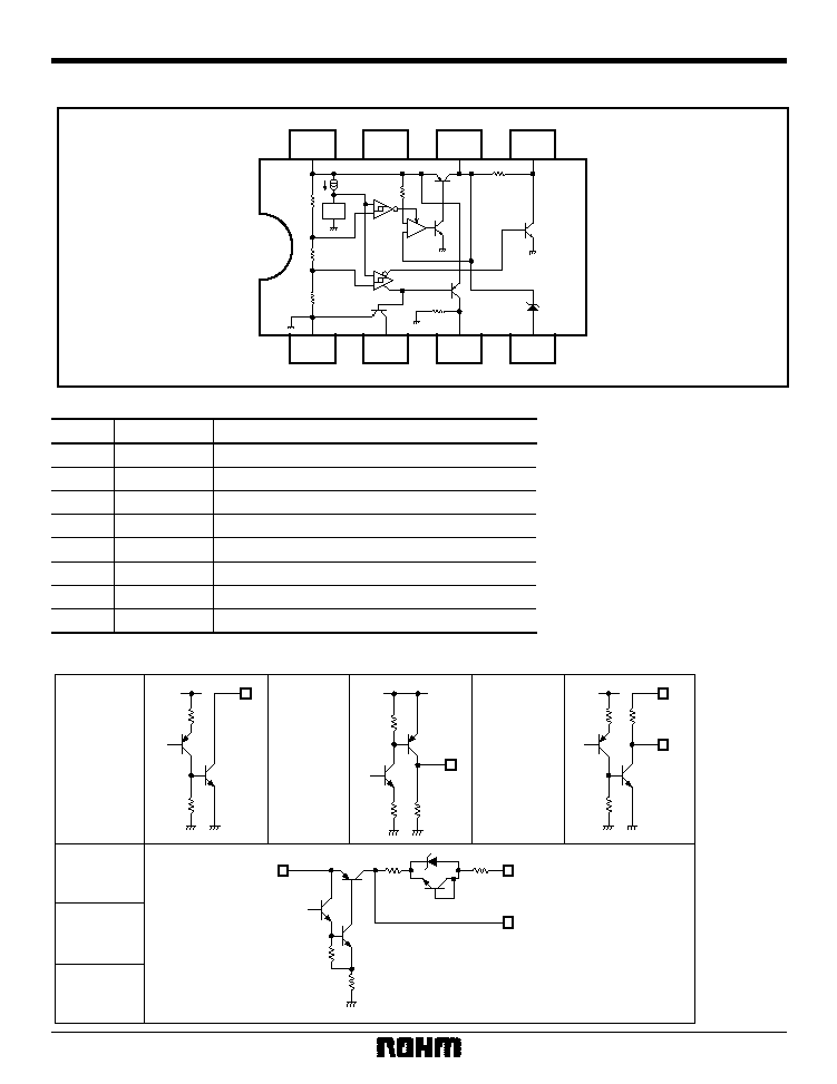
Input / output circuit
Pin 2
Reset
output
Pin 3
CS output
Pin 5
CSB output
Pin 6
Power supply
output
Pin 4
Battery
power supply
Pin 8
Power supply
(V
CC
)
Pin 6
Power supply
output
GND
2
6
GND
5
GND
GND
8
4
6
3
V
CC
V
CC
V
CC
·
Pin descriptions
Pin name
Function
1
GND
Substrate GND
2
Reset
Reset output
3
CS
CS output
4
Battery power supply
5
CSB
CSB output
6
V
O
Power supply output
7
8
Power supply voltage
V
BAT
V
CC
Pin No.
N.C.
--
·
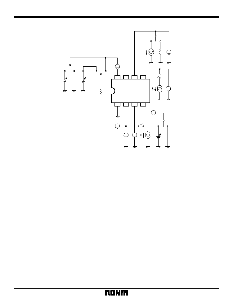
Block diagram
3
Memory ICs
BA6129AF / BA6162 / BA6162F
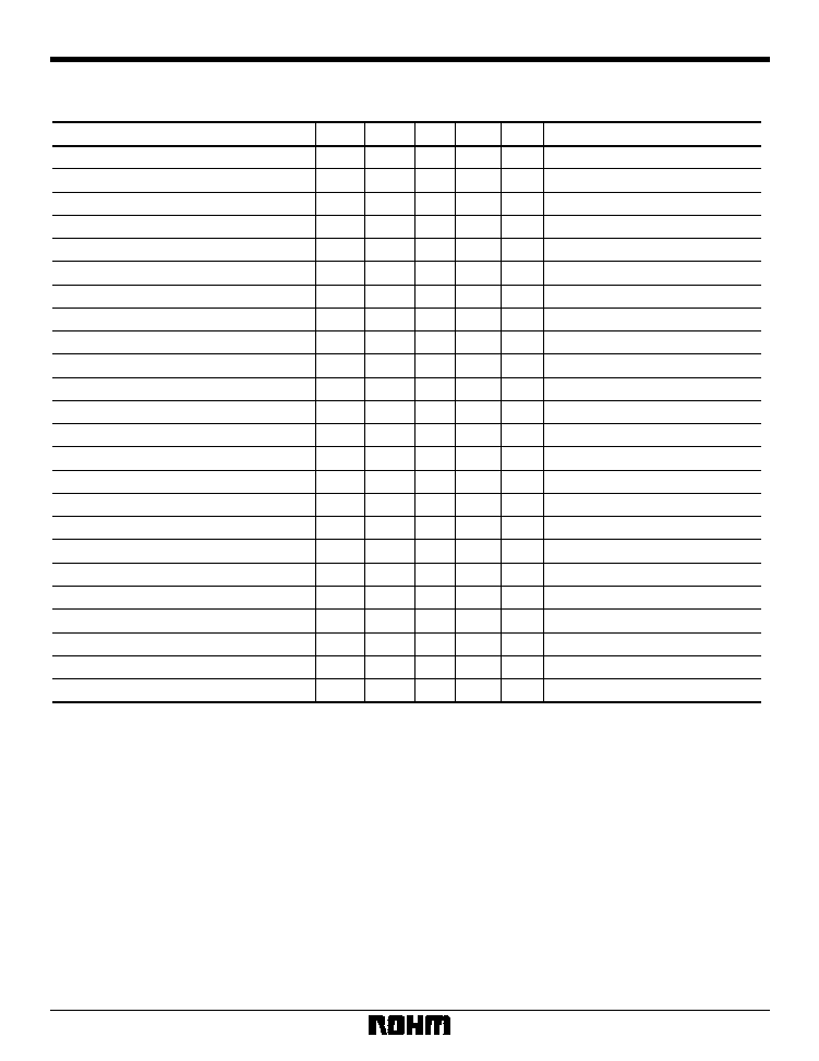
Parameter
Symbol
Min.
Typ.
Max.
Unit
Conditions
I
CC
--
--
2.0
mA
V
CC
= 5V, V
BAT
= 3V
V
SAT1
--
0.03
0.05
V
V
CC
= 5V, V
BAT
= 3V, I
O
= 1mA
V
O1
4.95
4.97
--
V
V
CC
= 5V, V
BAT
= 3V, I
O
= 1mA
V
O2
4.70
4.90
--
V
V
CC
= 5V, V
BAT
= 3V, I
O
= 15mA
V
O3
4.50
4.86
--
V
V
CC
= 5V, V
BAT
= 3V, I
O
= 30mA
V
S
3.35
3.50
3.65
V
V
CC
= H
L
V
SH
--
100
--
mV
V
CC
= L
H
V
RESL
--
--
0.4
V
V
CC
= 3V
I
RESH
--
--
0.1
µ
A
V
OPL
--
0.8
1.2
V
V
CC
= H
L, V
RES
0.4V
V
CSL
--
--
0.1
V
V
CC
= 3V, V
BAT
= 3V, I
CS
= + 1
µ
A
V
CSH
4.9
--
--
V
V
CC
= 5V, V
BAT
= 3V, I
CS
= 1
µ
A
V
CSBL
--
--
0.1
V
V
CC
= 5V, V
BAT
= 3V, I
CSB
= + 1
µ
A
V
CSBH
Vo 0.1
--
--
V
V
CC
= 3V, V
BAT
= 3V, I
CSB
= 1
µ
A
--
--
V
S
0.05
--
+ 0.05
% /
°
C
V
B
3.15
3.30
3.45
V
V
CC
= H
L, V
BAT
= 3V, R
O
= 200k
V
BH
--
100
--
mV
V
CC
= L
H, V
BAT
= 3V, R
O
= 200k
V
B
0.05
--
+ 0.05
% /
°
C
I
CCB
--
--
0.5
µ
A
V
CC
= GND, V
BAT
= 3V
V
SAT2
--
0.20
0.30
V
V
CC
= GND, V
BAT
= 3V, I
O
= 1
µ
A
V
O4
2.70
2.80
--
V
V
CC
= GND, V
BAT
= 3V, I
O
= 1
µ
A
V
O5
2.60
2.67
--
V
V
CC
= GND, V
BAT
= 3V, I
O
= 100
µ
A
I
OR
--
--
0.1
µ
A
V
CC
= 5V, V
BAT
= GND
V
CC
= 5V, VR
RES
= 7V
(Note) I
O
, I
CS
, and I
CSB
are + when flowing toward the pin and when flowing away from the pin.
Not designed for radiation resistance.
V
O6
V
CC
0.5
--
--
V
I
O
= 80mA
No-load current dissipation
I / O voltage differential 1
Vo output voltage 1
Vo output voltage 2
Vo output voltage 3
Detection voltage
Detection hysteresis voltage
Reset output low level voltage
Reset leakage current
Reset operating limit voltage
CS output low level voltage
CS output high level voltage
CSB output low level voltage
CSB output high level voltage
Detection voltage temperature characteristic
Switching voltage
Switching hysteresis voltage
Switching voltage temperature characteristic
Backup current dissipation
I / O voltage differential 2
Vo output voltage 4
Vo output voltage 5
Vo output voltage 6
Reverse current
·
Electrical characteristics
BA6129AF (unless otherwise noted, Ta = 25°C, VR
RES
= V
CC
= 5V, R
RES
= 10k
)
4
Memory ICs
BA6129AF / BA6162 / BA6162F
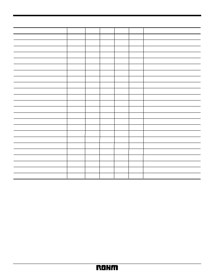
Parameter
Symbol
Min.
Typ.
Max.
Unit
Conditions
I
CC
--
--
2.0
mA
V
CC
= 5V, V
BAT
= 3V
V
SAT1
--
0.03
0.05
V
V
CC
= 5V, V
BAT
= 3V, I
O
= 1mA
V
O1
4.95
4.97
--
V
V
CC
= 5V, V
BAT
= 3V, I
O
= 1mA
V
O2
4.70
4.90
--
V
V
CC
= 5V, V
BAT
= 3V, I
O
= 15mA
V
O3
4.50
4.86
--
V
V
CC
= 5V, V
BAT
= 3V, I
O
= 30mA
V
S
4.00
4.20
4.40
V
V
CC
= H
L
V
SH
--
100
--
mV
V
CC
= L
H
V
RESL
--
--
0.4
V
V
CC
= 3.7V
I
RESH
--
--
0.1
µ
A
V
OPL
--
0.8
1.2
V
V
CC
= H
L, V
RES
0.4V
V
CSL
--
--
0.1
V
V
CC
= 3.7V, V
BAT
= 3V, I
CS
= + 1
µ
A
V
CSH
4.9
--
--
V
V
CC
= 5V, V
BAT
= 3V, I
CS
= 1
µ
A
V
CSBL
--
--
0.1
V
V
CC
= 5V, V
BAT
= 3V, I
CSB
= + 1
µ
A
V
CC
= 5V, VR
RES
= 7V
No-load current dissipation
I / O voltage differential 1
Vo output voltage 1
Vo output voltage 2
Vo output voltage 3
Detection voltage
Detection hysteresis voltage
Reset output low level voltage
Reset leakage current
Reset operating limit voltage
CS output low level voltage
CS output high level voltage
CSB output low level voltage
CSB output high level voltage
Detection voltage temperature characteristic
Switching voltage
Switching hysteresis voltage
Switching voltage temperature characteristic
Backup current dissipation
I / O voltage differential 2
Vo output voltage 4
Vo output voltage 5
Vo output voltage 6
Reverse current
V
CSBH
K
VS
V
B
V
BH
K
VB
I
CCB
V
SAT2
V
O4
V
O5
I
OR
V
O6
V
CC
= 3.7V, V
BAT
= 3V, I
CSB
= 1
µ
A
V
CC
= H
L, V
BAT
= 3V, R
O
= 200k
V
CC
= L
H, V
BAT
= 3V, R
O
= 200k
V
CC
= GND, V
BAT
= 3V
V
CC
= GND, V
BAT
= 3V, I
O
= 1
µ
A
V
CC
= GND, V
BAT
= 3V, I
O
= 1
µ
A
V
CC
= GND, V
BAT
= 3V, I
O
= 100
µ
A
V
CC
= 5V, V
BAT
= GND
I
O
= 40mA
Vo 0.1
0.05
3.15
--
0.05
--
--
2.70
2.60
--
V
CC
0.5
--
--
3.30
100
--
--
--
--
0.20
2.80
2.67
--
--
--
+ 0.05
3.45
--
+ 0.05
0.5
0.03
--
--
0.1
--
V
% /
°
C
V
mV
% /
°
C
µ
A
V
V
V
µ
A
V
(Note) I
O
, I
CS
, and I
CSB
are + when flowing toward the pin and when flowing away from the pin.
Not designed for radiation resistance.
BA6162 / F (unless otherwise noted, Ta = 25°C, VR
RES
= V
CC
= 5V, R
RES
= 10k
)
5
Memory ICs
BA6129AF / BA6162 / BA6162F
8
7
6
5
1
2
3
4
V
O
I
O
R
O
A
V
I
CSB
V
CSB
GND
A
V
V
A
10k
I
CC
VR
RES
V
CC
R
RES
I
RES
V
RES
V
CS
I
CS
V
BAT
I
CCB
.I
OR
BA6129AF
V
SAT
= V
CC
V
O
(V
B
)
(V
OPL
) (V
S
)
(V
S
.V
B
.V
OPL
)
(BA6162 / F)
200k
V
Fig. 1
·
Measurement circuit