∑
Block diagram
1
Standard ICs
6-channel high current driver
BA6256
The BA6256 is a low voltage, high current driver with six circuits, and is designed for applications such as LEDs,
relays, solenoids, and other driver devices which operate at low voltages. This driver is particularly ideal for direct
drive of CMOS controlled devices and other devices with a low input current of 5
µ
A (typ.).
1) Output current of 400mA (Max.) can be driven.
2) Equipped with strobe terminal.
3) High input impedance.
∑
Applications
Hammer solenoid drivers
Relay drivers
LED drivers
∑
Features
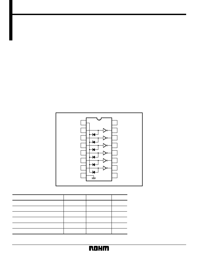
2
IN1
3
IN2
4
IN3
5
IN4
6
IN5
7
IN6
8
15
14
13
12
11
10
9
GND
OUT1
OUT2
OUT3
OUT4
OUT5
OUT6
Sub
N.C.
1
ST
16
V
CC
∑
Absolute maximum ratings (Ta = 25∞C)
Reduced by 5mW for each increase in Ta of 1
∞
C over 25
∞
C.
In this case, Tj = 15
∞
C.
Parameter
Symbol
Limits
Unit
Power supply voltage
V
CC
11
V
Power dissipation
Pd
500
mW
Input voltage
V
IN
≠ 0.5 ~ V
CC
V
Output current
I
O Max.
450
mA
Operating temperature
≠ 25 ~ + 75
∞
C
Storage temperature
≠ 55 ~ + 125
∞
C
Topr
Tstg
2
Standard ICs
BA6256
∑
Electrical characteristics (unless otherwise noted, Ta = 25∞C, Vcc = 6V)
Parameter
Symbol
Min.
Typ.
Max.
Unit
Conditions
Measurement
circuit
Usage voltage range
V
CC
3
6
10
V
--
Fig.4
Input high level voltage
V
IH
3
--
--
V
I
OUT
200mA, when only 1 circuit is on
Fig.4
Input low level voltage
V
IL
--
--
1
V
Fig.4
Output saturation voltage
V
CE (sat)
--
0.6
--
V
Fig.5
Output current (1 circuit)
I
OUT
--
--
400
mA
--
--
Input current
I
IN
--
5
--
µ
A
I
OUT
= 100mA, V
IN
= 6V
Fig.6
I
OUT
100
µ
A, when only 1 circuit is on
I
OUT
100
µ
A, when only 1 circuit is on
∑
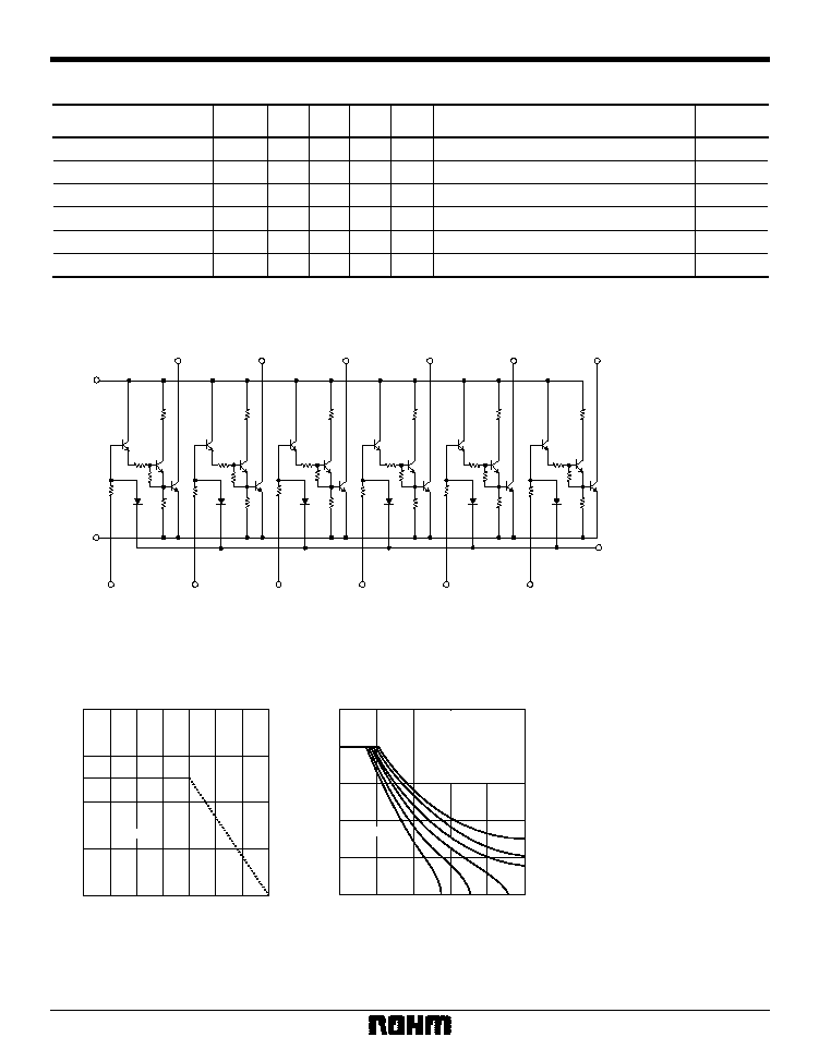
Internal circuit configuration
R
30
OUT6
R
23
10
R
22
R
24
R
21
D
6
Q
16
Q
17
Q
18
7
9
OUT5
R
19
11
R
18
R
20
R
17
D
5
Q
13
Q
14
Q
15
6
OUT4
R
15
12
R
14
R
16
R
13
D
4
Q
10
Q
11
Q
12
5
OUT3
Fig.1
R
11
13
R
10
R
12
R
9
D
3
Q
7
Q
6
Q
9
4
OUT2
R
7
14
R
6
R
8
R
5
D
2
Q
4
Q
5
Q
6
3
OUT1
R
3
15
16
R
2
R
25
R
26
R
27
R
28
R
29
R
4
R
1
D
1
Q
1
Q
2
Q
3
2
8
V
CC
1
ST.
IN6
IN5
IN4
IN3
IN2
IN1
N.C.
GND
R
1, 5, 9, 13, 17, 21
= 25k
R
2, 6, 10, 14, 18, 22
= 10k
R
3, 7, 11, 15, 19, 23
= 488
R
4, 8, 12, 16, 20, 24
= 6k
R
25, 26, 27, 28, 29, 30
= 40k
(Resistance values are typical values.)
∑
Electrical characteristic curves
600
400
200
0
0
≠ 25
25
50
75
100
AMBIENT TEMPERATURE : Ta (
∞
C)
POWER DISSIPATION : Pd (mW)
125
150
800
500mW
Fig.2 Power dissipation vs. ambient
temperature
500
400
300
200
100
0
20
0
40
60
80
100
DUTY CYCLE : (%)
MAXIMUM OUTPUT CURRENT : I
OUT
(mA)
V
CC
= V
IN
=
10V
9V
8V
6V
5V
Fig.3 Output current vs. duty cycle
When 6 circuits are
activated simultaneously
Repetition of 1 Hz min.
Ta = 75
∞
C max.
When V
CC
= V
IN
7V
