 | –≠–ª–µ–∫—Ç—Ä–æ–Ω–Ω—ã–π –∫–æ–º–ø–æ–Ω–µ–Ω—Ç: BA6267F | –°–∫–∞—á–∞—Ç—å:  PDF PDF  ZIP ZIP |
1
Standard ICs
Hex buffer / driver
BA6267 / BA6267F
The BA6267 and BA6267F can be connected with a high-voltage circuit such as the MOS and can be used to drive
high-current circuits such as lamps and relays. It can also be used as a buffer to drive TTL input.
∑
Applications
Drivers such as lamps and relays
TTL input buffers
∑
Features
∑
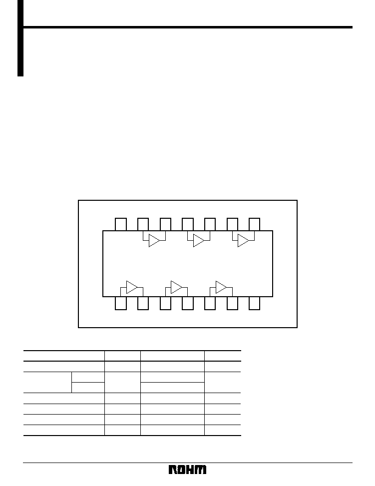
Block diagram
14
13
12
11
10
9
8
6
7
5
4
3
2
1
6A
6Y
5A
5Y
4A
4Y
1A
1Y
2A
2Y
3A
3Y
GND
BA6267 / BA6267F
V
CC
1) The pin layout is compatible with the SN7417.
2) Incorporates 6 circuits
∑
Absolute maximum ratings (Ta = 25∞C)
Parameter
Symbol
Limits
Unit
V
CC
7.0
V
BA6267
Pd
600
1
mW
BA6267F
550
2
Topr
0 ~ 70
∞
C
Tstg
≠ 55 ~ + 125
∞
C
V
I
≠ 0.3 ~ + 5.5
V
Vo
18
V
Applied voltage
Operating temperature
Storage temperature
Input voltage
Output terminal voltage
1 Reduced by 6.0mW for each increase in Ta of 1
∞
C over 25
∞
C.
2 Reduced by 5.5mW for each increase in Ta of 1
∞
C over 25
∞
C.
When mounted on a 50mm
◊
50mm
◊
1.6mm glass epoxy PCB.
Power dissipation
2
Standard ICs
BA6267 / BA6267F
∑
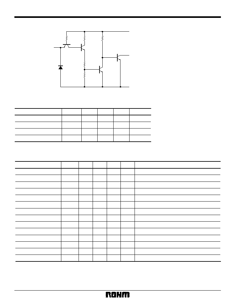
Input / output circuit
OUTPUT
GND
100
INPUT
V
CC
9k
3.4k
1.6k
1k
(Resistance values are typical values.)
∑
Recommended operating conditions
Parameter
Symbol
Min.
Typ.
Max.
Unit
4.75
5.0
5.25
V
2.0
--
--
V
--
--
0.8
V
--
--
15
V
V
CC
V
IH
V
IL
V
O
Power supply voltage
Input high level voltage
Input low level voltage
Output voltage
∑
Electrical characteristics (unless otherwise noted, Ta = 25∞C, Vcc = + 5.0V)
Parameter
Symbol
Min.
Typ.
Max.
Unit
Conditions
V
IH
2
--
--
V
V
IL
--
--
0.8
V
V
IH
--
15
40
µ
A
V
IL
--
≠ 0.33
≠ 1.6
mA
I
I
--
0.02
1
mA
V
IK
--
≠ 0.9
≠ 1.5
V
V
OL1
--
0.13
0.4
V
V
OL2
--
0.32
0.7
V
I
OH
--
2
250
µ
A
I
CCH
--
23
41
mA
I
CCL
--
16
30
mA
I
CC
--
3.25
6
mA
t
PLH
--
150
--
ns
t
PHL
--
20
--
ns
C
L
= 15pF, R
L
= 110
C
L
= 15pF, R
L
= 110
V
CC
= 5.25V, V
IH
= 2.4V
V
CC
= 5.25V, V
IL
= 0.4V
V
CC
= 5.25V, V
I
= 5.5V
V
CC
= 4.75V, I
I
= ≠ 12mA
V
CC
= 4.75V, I
OL
= 16mA
V
CC
= 4.75V, I
OL
= 40mA
V
CC
= 4.75V, V
OH
= 15V
Input high level voltage
Input low level voltage
Input high level current
Input low level current
Maximum input current
Input clamp voltage
Output saturation voltage
Output saturation voltage
Output leakage current
Supply current 1
Supply current 2
Supply current 3
Output delay time 1
Output delay tim 2
Total current when all outputs at "H"
Total current when all outputs at "L"
Average current per gate when the duty cycle is 50%
--
--
3
Standard ICs
BA6267 / BA6267F
∑
Measurement conditions
OUTPUT
R
L
C
L
TEST POINT
V
CC
Fig.1 Load circuit
3V
0V
V
OH
V
OL
1.5V
1.5V
1.5V
1.5V
INPUT
t
PLH
t
PHL
OUTPUT
Fig.2 Output delay time
∑
Electrical characteristic curves
600
0
≠ 25
500
400
300
200
100
25
50
75
100
125
0
BA6267
BA6267F
AMBIENT TEMPERATURE : Ta (
∞
C)
POWER DISSIPATION : Pd (mW)
Fig.3 Power dissipation vs. ambient
temperature
BA6267F
BA6267
50
40
30
20
10
20
40
60
80
100
0
0
DUTY CYCLE (%)
OUTPUT CURRENT : I
OL
(mA)
Fig.4 Output conditions
∑
External dimensions (Units: mm)
BA6267
BA6267F
DIP14
SOP14
6.5
±
0.3
19.4
±
0.3
0.5
±
0.1
3.2
±
0.2
4.25
±
0.3
14
8
7
1
0.3
±
0.1
0.51Min.
7.62
0
∞
~ 15
∞
2.54
0.4
±
0.1
1.27
1
14
8.7
±
0.2
7
8
4.4
±
0.2
6.2
±
0.3
0.11
1.5
±
0.1
0.15
0.15
±
0.1
0.3Min.