 | –≠–ª–µ–∫—Ç—Ä–æ–Ω–Ω—ã–π –∫–æ–º–ø–æ–Ω–µ–Ω—Ç: BA6438S | –°–∫–∞—á–∞—Ç—å:  PDF PDF  ZIP ZIP |

BA6438S
Motor driver ICs
3-phase motor driver
BA6438S
The BA6438S is a 3-phase, full-wave, pseudo-linear motor driver suited for VCR capstan motors. The IC has a torque
ripple cancellation circuit to reduce wow and flutter, and an output transistor saturation prevention circuit that provides
superb motor control over a wide range of current. The built-in motor power switching regulator allows applications with
low power consumption
!Applications
3-phase VCR capstan motors
!Features
1) 3-phase, full-wave, pseudo-linear drive system.
2) Torque ripple cancellation circuit.
3) Reversal brake based on the detection of motor
direction.
4) Output transistor (high-and low-sides) saturation
5) Motor power switching regulator with oscillation circuit.
6) Output-to-GND short-circuit detection.
7) Available in SDIP 24-pin power package (with radiation
fins).
prevention circuit
!Absolute maximum ratings
(Ta = 25
∞C)
Parameter
Symbol
Limits
Unit
V
CC
7
V
V
M
24
V
Pd
2000
1
mW
Topr
-
10
+
75
∞
C
Tstg
-
40
+
150
I
Opeak
1.7
2
A
1 Reduced by 16mW for each increase in Ta of 1
∞
C over 25
∞
C.
Applied voltage
Applied voltage
Power dissipation
Operating temperature
Storage temperature
Allowable output current
2 Should not exceed the ASO value.
∞
C
!Recommended operating conditions
(Ta = 25
∞C)
Parameter
Symbol
Min.
Typ.
Max.
Unit
V
CC
4
5
6
V
V
M
3
12
23
V
Operating power supply voltage
Operating power supply voltage
BA6438S
Motor driver ICs
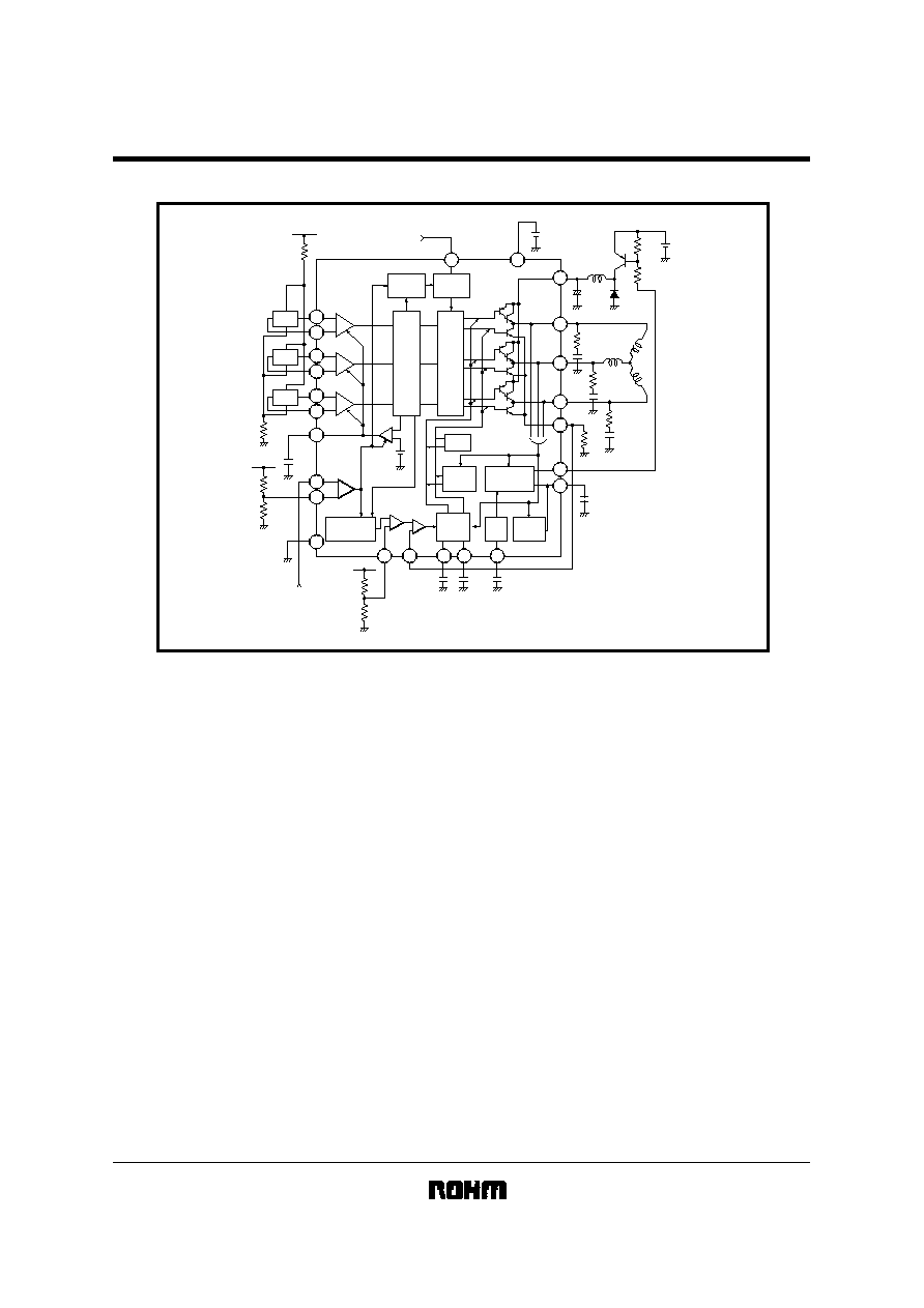
!Block diagram
TSD
RIPPLE
CANCELLATION
TORQUE
COMMAND
SHORT
CIRCUIT
DET.
SWITCHING
REGULATOR
OSC
10
9
H1
+
Hall
Amp.
Hall
8
7
H1
-
H2+
H2
-
6
5
H3+
H3
-
AGC
4
17
16
12
20
22
18
21
15
14
13
2
1
3
23
24
19
P
C
H
V
CC
E
C
E
CR
P
C
V
P
C
I
OSC
VS
REG
ATC
A3
A2
A1
V
M
V
CC
ED / S
CONTROL
SIGNAL
SIGNAL V
CC
MOTOR V
CC
V
CC
GND
TL
CS
OUTPUT
SATURATION
OUTPUT
SATURATION
MOTOR
DIRECTION
DET
MOTOR
DIRECTION
SETTING
11
Hall
Hall
P SIGNAL COMBINER
MOTOR DIRECTION SWITCHING

BA6438S
Motor driver ICs
!Pin descriptions
Pin No.
1
A3
2
ATC
3
A2
4
PCH
5
H3
-
6
H3
+
7
H2
-
8
H2
+
9
H1
-
10
H1
+
11
12
GND
13
REG
14
V
S
15
OSC
16
ECR
17
EC
18
PCV
19
V
CC
20
TL
21
PCI
22
CS
23
A1
24
V
M
ED / S
Pin name
Function
Motor output
Driver ground
Motor output
Hall amplifier AGC phase compensation
Hall signal input
Hall signal input
Hall signal input
Hall signal input
Hall signal input
Hall signal input
Signal ground
Switching regulator output (sink output)
High-side saturation detection output
Oscillator capacitor connection
Torque control reference voltage input
Torque control signal input
Phase compensation for preventing driver high-side saturation
Signal power supply
Torque limiter
Phase compensation for preventing driver low-side saturation
Current sensing input
Motor output
Motor power supply
Forward when LOW; stop when MEDIUM; reverse when HIGH
!Electrical characteristics
(unless otherwise noted, Ta = 25
∞C, V
CC
= 5V, V
M
= 12V)
Parameter
Symbol
Min.
Typ.
Max.
Unit
Conditions
G
io
0.25
0.31
0.36
-
E
C
=
2.2
2.1V,
Input
=
L, L, H
V
RCC
4.6
6.4
7.2
%
V
OH
1.1
1.5
1.9
V
I
O
=
0.8A
V
OL
0.95
1.3
1.65
V
I
O
=
0.8A
f
OSC
100
135
160
kHz
C
=
470pF
G
us
5.0
6.5
8.0
-
-
I
REGO
30
-
-
mA
V
O
=
5V
Input
=
L, L, H
L, M, H
Not designed for radiation resistance.
Torque control input / output gain
Ripple cancel ratio
Output high level voltage
Output low level voltage
Oscillator frequency
Saturation detection output gain
Regulator current capacity
BA6438S
Motor driver ICs
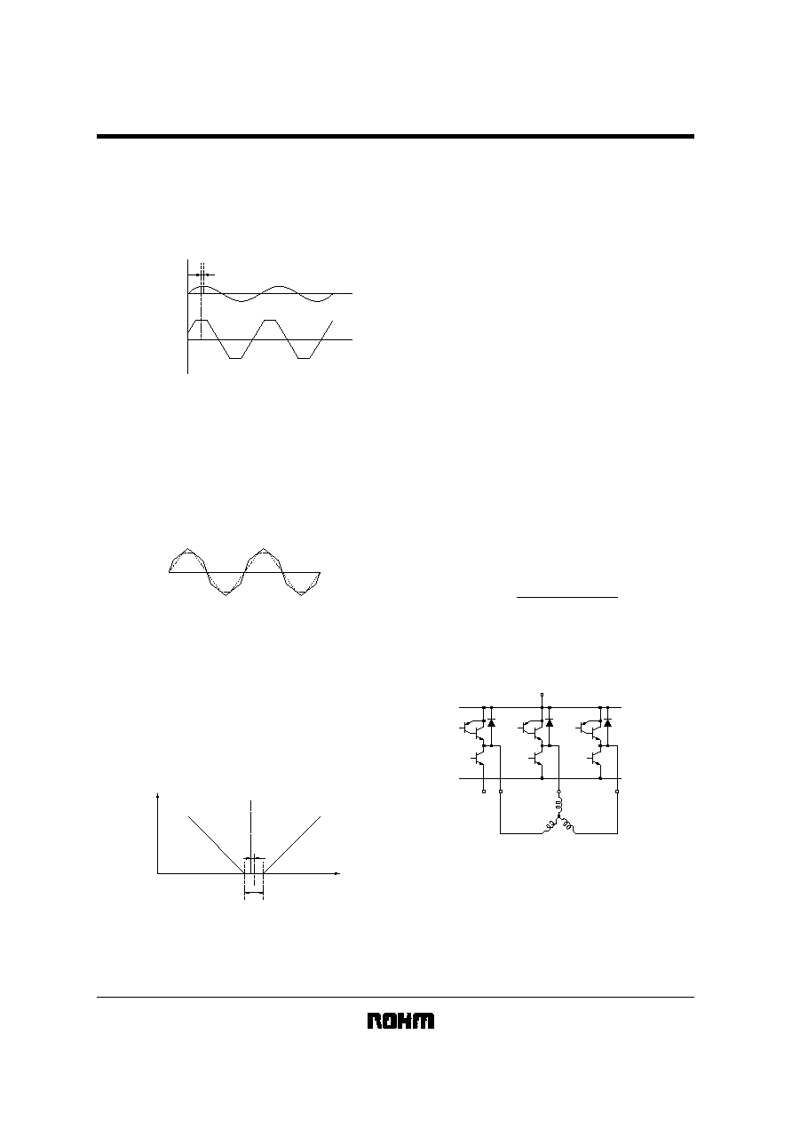
!Circuit operation
(1) Pseudo-linear output and torque ripple cancellation
The IC generates a trapezoidal (pseudo-linear) output
current, whose waveform phase is 30 degrees ahead of
that of the Hall input voltage (Fig. 1).
.
30
∞
Hall input
Output current
Fig. 1
The trapezoidal waveform of output current would create
intermittence in the magnetic field generated by the 3-
phase motor, and would result in an irregular rotation of
the motor. To prevent this, the output waveform is ob-
tained by superimposing a triangular wave on the trape-
zoidal wave (Fig. 2). This process is called torque ripple
cancellation.
Fig. 2
(2) Torque control and reversal brake
The output current can be controlled by adjusting the
voltage applied to the torque control pins (pins 16 and 17).
These pins are the inputs to a differential amplifier. A ref-
erence voltage between 2.3 ~ 3.0V (2.5V recommended)
is applied to pin 16.
0
Output current
Offset
Pin 16
reference voltage (2.5 V)
Pin 17 voltage
Dead zone (100 mV typically)
Fig. 3
A brake is applied to the motor as described in the
following.When the motor is running, pin 17 is given a
negative potential with respect to the reference potential. If
the pin 17 potential becomes positive, the IC detects the
rise of pin 17 potential above the reference potential and
activates the motor direction detecting circuit.
The motor direction detecting circuit sends a signal to the
motor direction setting circuit to reverse the motor direc-
tion. This causes a braking torque that depends on the
pin 17 potential, so that the motor quickly reduces its
speed. At the same time, the positive pin 17 potential is
shifted to the reference potential, so that the motor stops
smoothly.
(3) Output current sensing and torque limitation
Pin 2 is the ground pin for the output stage. To sense the
output current, a resistor (0.5
recommended) is con-
nected between pin 2 and the ground. The output current
is sensed by applying the voltage developed across this
resistor to pin 22 as a feedback.
The output current can be limited by adjusting the voltage
applied to pin 20. The current is limited when pin 20
reaches the same potential as pin 22. The output current
(I
MAX
. ) under this condition is given by:
I
MAX
.
=
V
20P(
TL
-
CS
ofs
)
R
2P
where R
2P
is the value of the resistor connected between
pin 2 and the ground, V
20P
is the voltage applied to pin 20,
and (TL≠CS
ofs
) is the offset between the TL and CS pins.
24pin
1pin
3pin
23pin
ATC
2pin
V
M
Fig.4 Output circuit
BA6438S
Motor driver ICs
(4) Motor direction control (pin 11)
The motor mode is :
Forward when the pin 11 voltage is less than 0.9V,
Stop when the voltage is between 1.3
~
3.0V,
Reverse when the voltage is above 3.5V.
In the stop mode, high-and low-side output transistors
are turned off, resulting in a high impedance state.
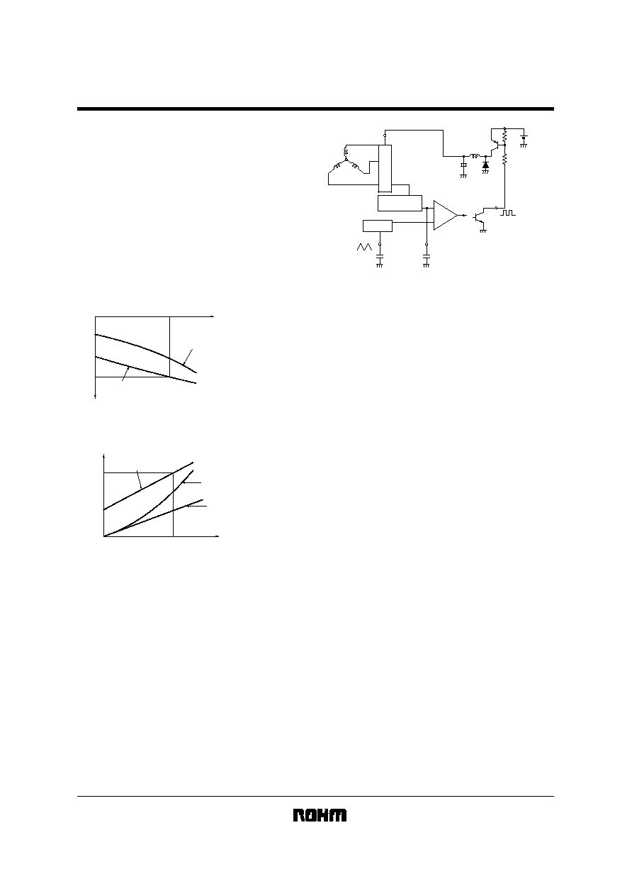
(5) Output transistor saturation prevention circuit
This circuit monitors the output voltage and maintain the
operation of the output transistors below their saturation
levels. Operating the transistors in the linear characteristic
range provides good control over a wide range of current
and good torque characteristics even during overloading.
800mA
1.5V
0
Output current
Output
saturation
voltage
HIGH level voltage
HIGH level output voltage
Fig.5 High level output voltage vs.
output current (reference curves)
800mA
0
1.3V
Output current
Output saturation voltage
LOW level output voltage
LOW level voltage
ATC-pin voltage
Fig.6 Low level output voltage vs. output
current (reference curves)
(6) Switching regulator
The BA6438S has a switching regulator output pin. The
IC outputs a PWM signal by comparing the output of the
internal oscillator with the HIGH level output voltage
monitored.
24
13
14
15
OSC
V
S
REG
+
V
M
Driver
Fig. 7
HIGH level
voltage monitor
Oscillator
As shown in Fig. 7, the switch regulator circuit reduces the
power consumed by the IC by reducing the collector-to-
emitter (C-E) voltage of the driver transistors.
Nearly all the power dissipated by the IC is dissipated be-
tween the collectors and emitters of the output transistors.
More power is consumed as the C-E voltage increases and
as the output current increases.
The output transistor C-E voltage is equal to the difference
between the supply voltage and the voltage applied to the
motor. Because the voltage across the motor decreases with
decreasing drive current, the C-E voltage must increase if the
supply voltage is fixed.
Therefore, to improve the efficiency of the driver and to
prevent the power rating of the IC being exceeded, the supply
voltage must be varied in response to changes in the output
current. The supply voltage is decreased at low current and
increased at high current so that no excessive voltage is
applied between the transistor collectors and emitters .
(7) Output-to-ground short-circuit detection
The motor output pins of the IC may be short-circuited to the
ground by some fault conditions. A short-circuited output can
destroy the output transistors because of excessive current,
excessive voltage, or both. Even when a short-circuit
condition does not completely destroy the device, it can still
cause extreme overheating. To prevent this, the BA6438S
contains a short-circuit detection circuit that turns off the motor
drive current if the output-to-ground potential becomes
abnormally low.