706
Motor driver ICs
2-phase half-wave motor driver
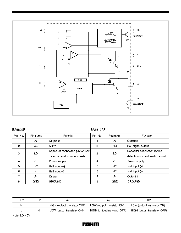
BA6809F / BA6819AF
The BA6809F and BA6819AF are motor drivers designed for 3V and 5V fan motors. Built-in output transistors reduce
the number of external components required. The ICs have an alarm output pin (BA6809F) and Hall output pin
(BA6819AF).
F
Applications
Fan motors
F
Features
1) Lock detection and rotational speed sensing mecha-
nisms are built in.
2) Alarm output pin (BA6809F) and Hall output pin
(BA6819AF).
3) Built-in thermal shutdown circuit.
4) Operation assured with a supply voltage as low as
2.7V.
5) Compact 8-pin SOP package.
F
Absolute maximum ratings (Ta = 25
_
C)
F
Recommended operating conditions (Ta = 25
_
C)
709
Motor driver ICs
BA6809F / BA6819AF
F
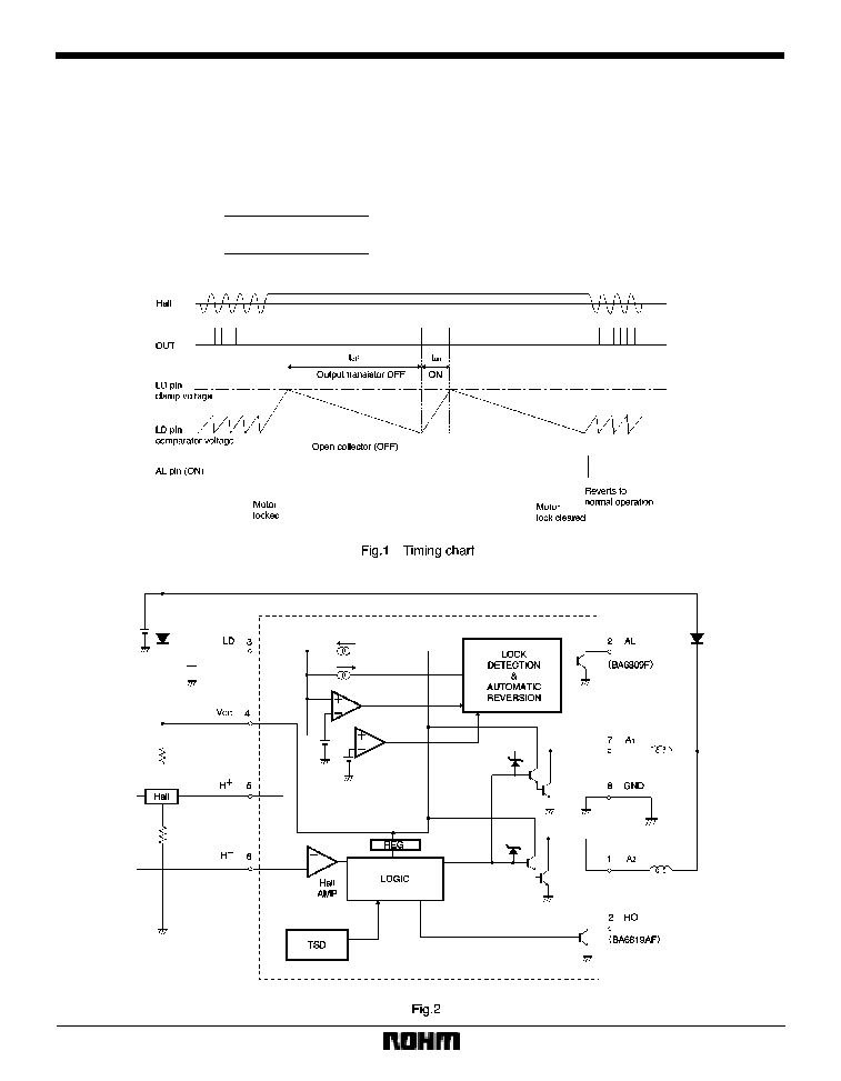
Circuit operation
The BA6809F and BA6819AF have motor lock detection
and automatic restart circuits. The timing of lock detec-
tion and automatic restart is determined by the external
capacitor connected to the LD pin. The charge time of the
external capacitor is given by :
(Typical value)
where
V
LDCL
is the LD-pin clamp voltage
(1.90V),
V
LDCP
is the LD-pin comparator voltage
(0.73V),
I
LDC
is the LD-pin charge current
(2.2
�
A),
I
LDD
is the LD-pin discharge current
(0.42
�
A),
C is the capacitance of the LD-pin external capacitor.
For C=0.47
�
F, for example, the charge and discharge
times are 0.25s (output ON) and 1.31s (output OFF), re-
spectively.
F
Application example
I
LDC
t
on
(Charge time)=
C
S
(V
LDCL
*
V
LDCP
)
I
LDD
t
off
(Discharge time)=
C
S
(V
LDCL
*
V
LDCP
)
710
Motor driver ICs
BA6809F / BA6819AF
F
Operation notes
(1)
Thermal shutdown circuit
The IC has a built-in thermal shutdown circuit. The is a
temperature difference of 20
_
C (typical) between the
temperatures at which the circuit is activated and deacti-
vated.
The circuit is activated at the temperature of about 175
_
C
(typical), so that all outputs are turned OFF. Normal op-
eration resumes when the circuit is deactivated.
(2)
Power dissipation
Power consumed in the IC can be calculated from the fol-
lowing equation :
P
C
=P
C1
)
P
C2
)
P
C3
P
C1
is power consumed by the circuit current.
P
C1
=V
CC
I
CC
P
C2
is the output current consumption.
P
C2
=V
OL
I
O
V
OL
is the LOW level output voltage of output pins
1 and 2, and I
O
is the sink current of pins 1 and 2.
P
C3
is power consumed by the AL and HO pins.
P
C3
=V
ALL
I
AL
(BA6809F)
P
C3
=V
HOL
I
HO
/ 2 (BA6819AF)
where
V
ALL
is the AL-pin LOW level voltage,
I
AL
is the AL-pin sink current,
V
HOL
is the HO-pin LOW level voltage,
I
HO
is the HO-pin sink current.
Make sure that your application does not exceed the al-
lowable power dissipation of the IC.
(3)
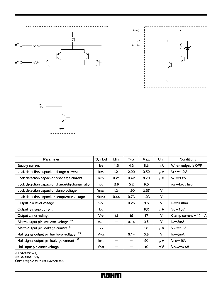
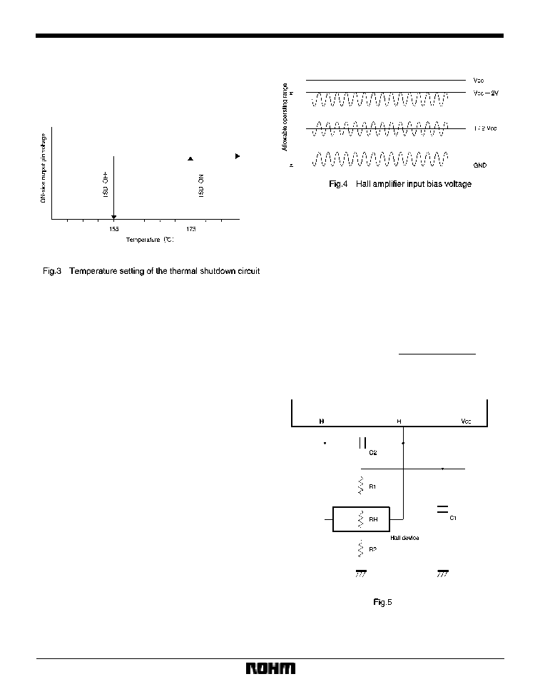
Hall amplifier input voltage
The R1 and R2 resistances must be set so as to maintain
the Hall amplifier input bias voltage within the range of 0V
to (V
CC
*
2V) including the signal amplitude.
The Hall device may be affected by power supply noise
due to the PCB conductor pattern. If you have this prob-
lem, insert a capacitor C1 as shown in Fig. 5.
If the conductor lines from the Hall device output termi-
nals to the Hall inputs of the IC are particularly long, noise
can be picked up and fed into the inputs. If you have this
problem, insert a capacitor C2 as shown in Fig. 5. Note
that the Hall inputs have no hysteresis in this IC.
where RH is the Hall device impedance.
R1
)
R2
)
RH
Hall current is given by=
V
CC