 | ÐлекÑÑоннÑй компоненÑ: BA6908F | СкаÑаÑÑ:  PDF PDF  ZIP ZIP |
Äîêóìåíòàöèÿ è îïèñàíèÿ www.docs.chipfind.ru

BA6908F
Motor driver ICs
1/7
Single-phase full-wave motor driver for
fan motor
BA6908F
BA6908F is a single phase full-wave motor driver for fan motor corresponding to 5V and 12V. Switching noise is reduced
by soft switching drive. This IC has lock detection and automatic restart functions as motor protection function.
Applications
Motor drivers for fan motors
Features
1) Single-phase full-wave drive system.
2) Built-in power transistor.
3) Soft switching drive.
4) Lock detection and automatic restart circuit.
5) Thermal shut-down circuit.
6) Hall signal output.
Absolute maximum ratings (Ta=25
°
C)
Parameter
Symbol
Limits
Unit
Supply voltage
V
CC
I
OUT
I
HO
V
OUT
V
HO
Tjmax
15
15
15
15
150
1
2
0.7
V
V
V
A
mA
Power dissipation
Pd
687
mW
Storage temperature
Topr
°
C
°
C
°
C
Output current
Hall signal output current
Output voltage
Junction temperature
Hall signal output voltage
Operating temperature
Tstg
1 To use at temperature above Ta
=
25
°
C reduce 5.5mW/
°
C.
(On 70.0mm
×
70.0mm
×
1.6mm glass epoxy board)
2 This value is not to be over Pd and ASO.
-
40 to
+
85
-
55 to
+
150
Recommended operating conditions (Ta=25
°
C)
Parameter
Symbol
Min.
Typ.
Max.
Unit
Supply voltage
V
CC
3
-
14
V
BA6908F
Motor driver ICs
2/7
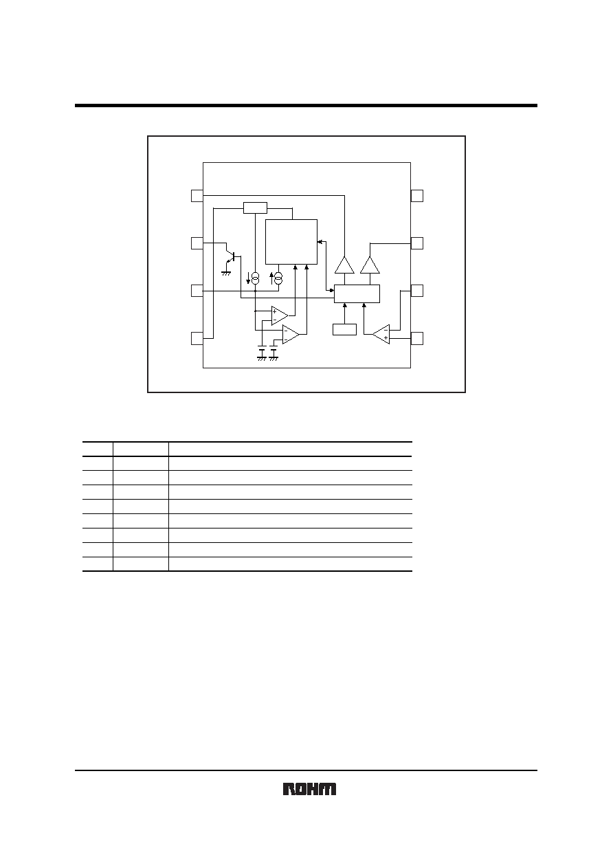
Block diagram
1
2
3
4
8
7
6
5
REG
TSD
LOCK
DETECTION
AND
AUTO RESTART
Control
HALL
AMP
Terminal function table
Pin name
Function
Pin No.
1
2
3
4
5
6
7
8
OUT2
HO
LD
H
-
GND
GROUND terminal
V
CC
Hall signal input terminal
+
Hall signal output terminal
Connection terminal of capacitor for lock detection, auto restart
Power supply terminal
Output terminal 2
Hall signal input terminal
-
Output teminal 1
H
+
OUT1
BA6908F
Motor driver ICs
3/7
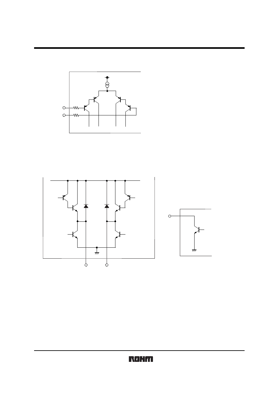
Input / output circuit
<Hall input>
V
CC
H
+
H
-
Fig.1
<Coil output> <HO output>
OUT1
OUT2
V
CC
Fig.2
HO
Fig.3
BA6908F
Motor driver ICs
4/7
Electrical characteristics (Unless otherwise specified, Ta=25
°
C, V
CC
=5V)
Parameter
Symbol
Min.
Typ.
Max.
Unit
Conditions
Supply current
Charge current of capacitor for lock detection
Discharge current of capacitor for lock detection
Charge-discharge current ratio of capacitor for lock detection
Comparison voltage of capacitor for lock detection
Output voltage L
Output voltage H
Clamp voltage of capacitor for lock detection
I
CC
ILDC
ILDD
VOL
VOH
rCD
VLDCL
VLDCP
1.5
1.50
4.2
320
500
680
-
1.14
0.47
0.3
-
3.4
2.75
8.7
4.50
0.24
0.48
0.90
5.7
9.5
1.80
-
3.9
0.76
2.47
0.2
4.1
1.06
mA
µ
A
-
V
V
V
"HO" terminal voltage L
"HO" terminal leak current
VHOL
IHOL
0.5
-
-
0.3
0
50
V
µ
A
µ
A
V
At output : OFF
VLD
=
1.1V
VLD
=
1.1V
VHO
=
15V
rCD
=
ILDC/ILDD
IHO
=
5mA
Hall input offset voltage
Hall input-output gain
Hofs
GHO
10
-
10
-
mV
I
O
=
200mA
I
O
=
200mA
This product is not designed for protection against radioactive rays.
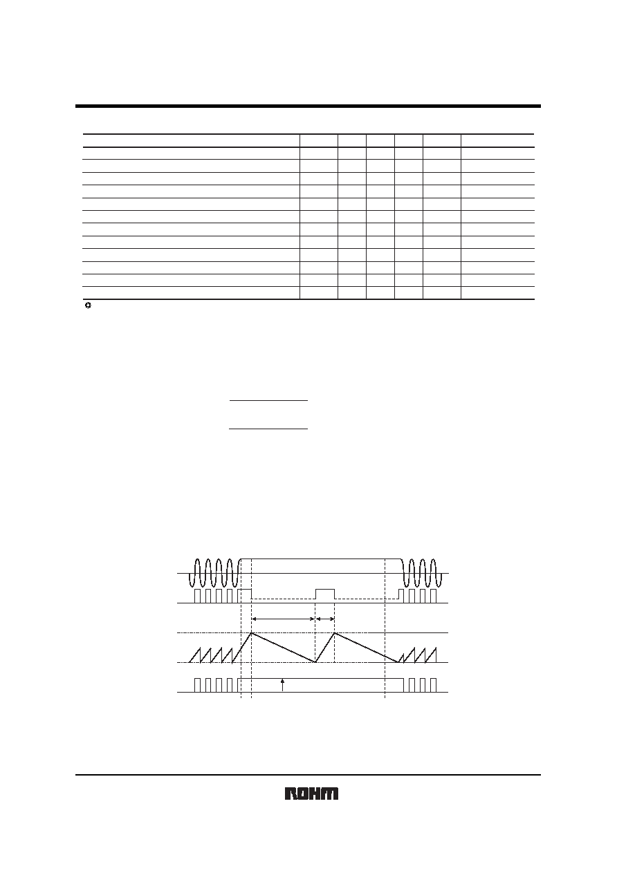
Lock detect circuit, automatic restart circuit
Charge and discharge time at motor lock condition varies with the value of external capacitor at LD terminal and is
given by the following equation.
Ton (Charge time)
=
ILDC
C· (VLDCL-VLDCP)
Toff (Discharge time)
=
ILDD
C· (VLDCL-VLDCP)
C
VLDCL
VLDCP
ILDC
ILDD
:
:
:
:
:
(1.80V Typ.)
(0.76V Typ.)
(2.75
µ
A Typ.)
(0.48
µ
A Typ.)
The following value shows charge time and discharge time at C
=
0.47
µ
F for reference.
Charge time
=
0.18SEC (Output : ON)
Discharge time
=
1.02SEC (Output : OFF)
Value of capacitor at LD terminal
Clamp voltage of capacitor lock detection
Comparison voltage of capacitor lock detection
Charge current of capacitor lock detection
Discharge current of capacitor lock detection
Toff
Output Tr OFF
VLDCL
Motor lock
Detect lock
Lock cancel
Depend on the hall output
Reset ordinary motion
H
+
OUT1
LD
HO
VLDCP
ON
Ton
Fig.4 Timing chart
BA6908F
Motor driver ICs
5/7
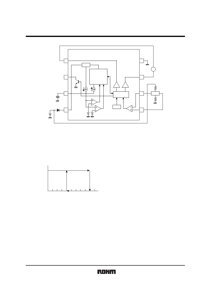
Application circuit
1
2
3
4
8
7
6
5
REG
TSD
LOCK
DETECTION
AND
AUTO RESTART
Control
HALL
AMP
HALL
M
Fig.5
Cautions
1) Thermal shut down(TSD)
This IC is built-in TSD.
TSD has the temperature hysteresis.
Fig.6 TSD
Output ON
Output OFF
TSD OFF
TSD ON
150
175
Junction temperature(
°
C)
TSD ON (Typ. : 175
°
C)
All output transistor OFF.
TSD OFF (Typ. : 150
°
C)
Reset ordinary motion.
(It has the temperature hysteresis
of 25
°
C
<
TYP
>
)
2) Power
dissipation
IC power dissipation widely varies with supply voltage, output current and application of IC. Please be careful for the
thermal design not to exceed the allowable power dissipation.
Document Outline