594
Motor driver ICs
2-phase motor driver for VCR cylinder
motors
BA6970FS
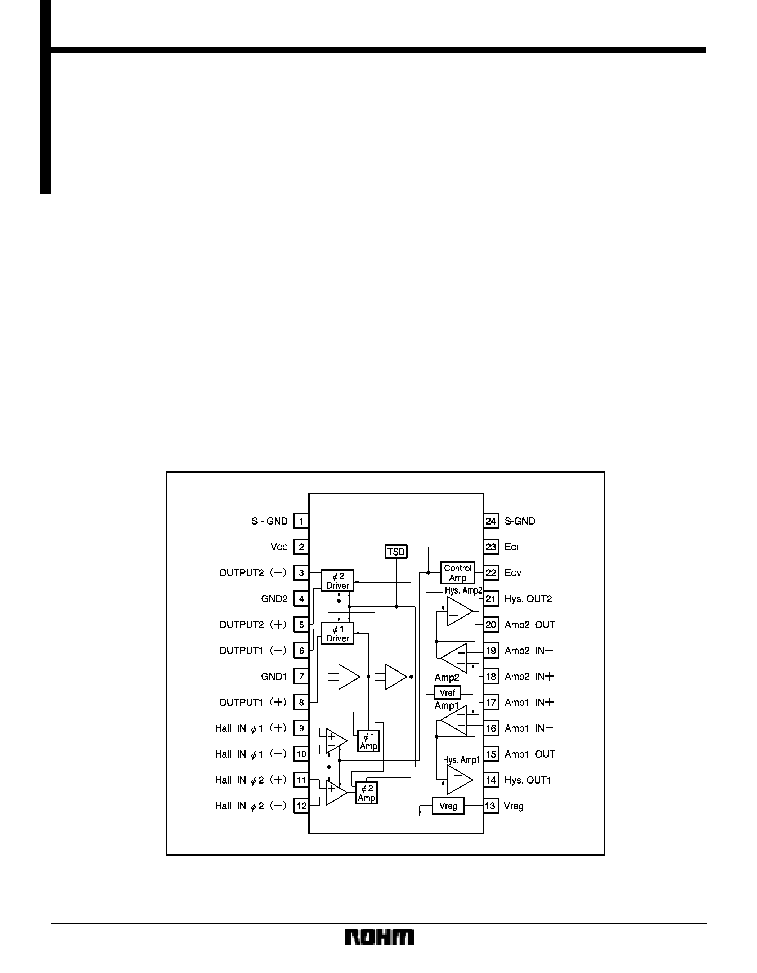
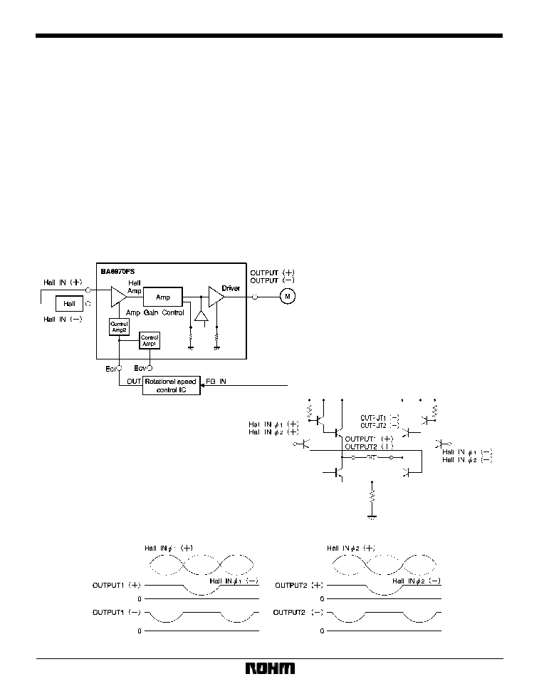
The BA6970FS is a direct-drive motor driver suitable for 2-phase, full-wave linear motors. The IC consists of a Hall ampli-
fier control circuit, driver circuits, FG / PG signal amplifiers, and hysteresis amplifiers.
F
Applications
VCR cylinder motors
F
Features
1) Linear drive system provides low switching noise.
2) Output current can be controlled by either current or
voltage input.
3) Two amplifiers and two hysteresis amplifiers.
4) Constant supply voltage pin for hall devices.
5) High ratio of output current and control current.
(4000 typically)
6) Available in a compact surface-mount package.
F
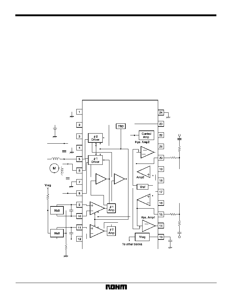
Block diagram
595
Motor driver ICs
BA6970FS
F
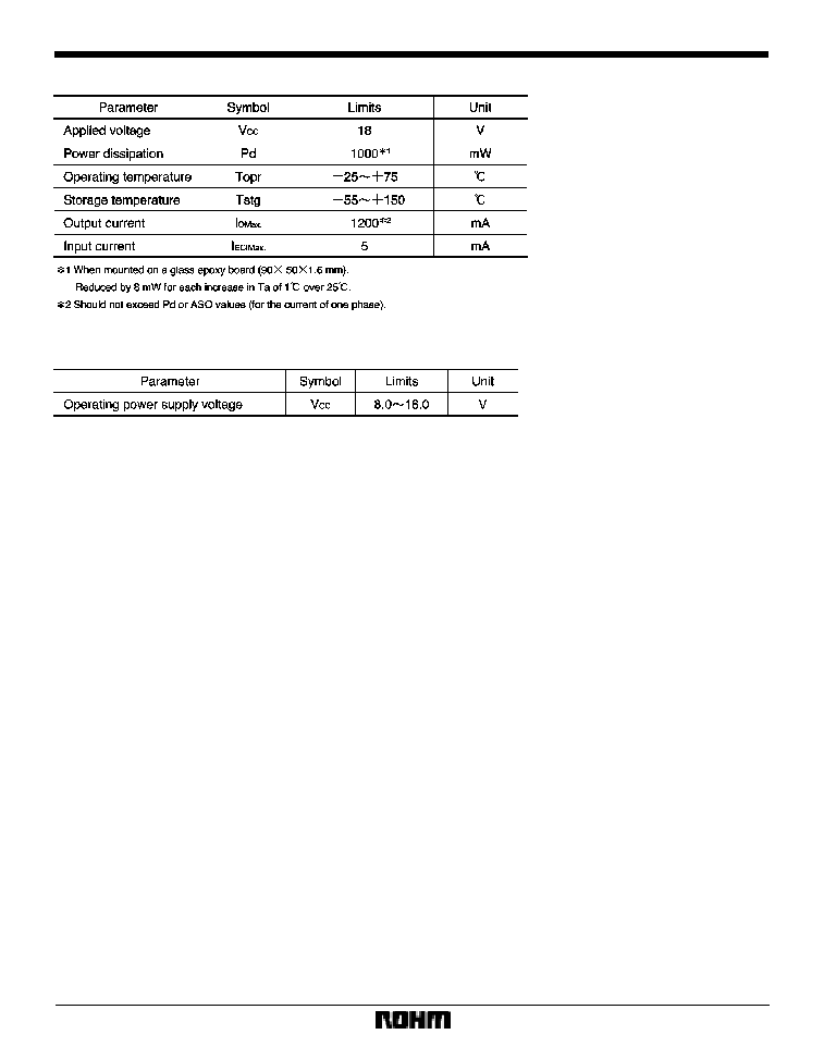
Absolute maximum ratings (Ta = 25
_
C)
F
Recommended operating conditions (Ta = 25
_
C)
596
Motor driver ICs
BA6970FS
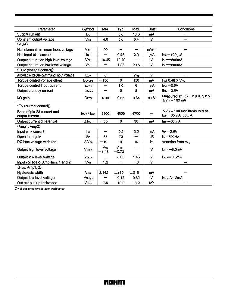
F
Electrical characteristics (unless otherwise noted, Ta = 25
_
C, V
CC
= 12V)

597
Motor driver ICs
BA6970FS
F
Pin descriptions
598
Motor driver ICs
BA6970FS
F
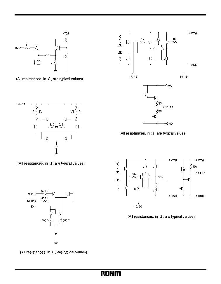
Input / output circuits
(1)
E
CV
(22 pin)
(2)
Coil output (8, 6, 5, 3 pin)
(3)
Hall inputs (9, 10, 11, 12 pin), E
CI
input
(4)
I / O of amplifiers 1 and 2
(5)
I / O of hysteresis amplifiers
Note that the resistance values can vary
�
30%
Fig.1
Fig.2
Fig.3
Fig.4
Fig.5
599
Motor driver ICs
BA6970FS
F
Circuit operation
(1)
The signal from the Hall device is amplified by the
Hall amplifier and then supplied to the driver circuit. The
driver gain, which is constant, is regulated by changing
the Hall amplifier gain with the E
CI
input current or the E
CV
input voltage (E
CI
and E
CV
are output current control pins).
The motor rotational speed is sensed by the FG, and the
output from which is F / I-converted and supplied to the
E
CI
pin or F / V-converted and supplied to the E
CV
pin as
a feedback signal, so that a constant rotational speed is
maintained as follows (Fig. 6) :
(
1) The motor speed decreases.
(
2) The speed control IC outputs a feedback signal
(
3) The Hall amplifier gain increases.
(
4) The output current increases.
(
5) The motor speed increases.
(2)
When the voltage on Hall IN
1
(
)
) is higher than the
voltage on Hall IN
1
(
*
), an output current flows from
OUT1 (
)
) to OUT1 (
*
) according to the voltage differen-
tial. When the voltage on Hall IN
1
(
*
) is higher, on the
other hand, an output current flows from OUT1 (
*
) to
OUT1 (
)
).
Similarly, when the voltage on Hall IN
2
(
)
) is higher than
the voltage on Hall IN
2
(
*
), an output current flows from
OUT2 (
)
) to OUT2 (
*
) according to the voltage differen-
tial. When the voltage on Hall IN
2
(
*
) is higher, on the
other hand, an output current flows from OUT2 (
*
) to
OUT2 (
)
).
Fig.6
Fig.7
Fig.8

600
Motor driver ICs
BA6970FS
(3)
Output waveforms are shown in Fig. 9. Because of
the amplifier offset, the output is left OPEN when the out-
put signal switches from positive to negative. The output
waveform is determined by the external circuit because
the IC impedance increases during this transition period.
Since inductive loads are usually provided, a capacitor
should be connected to suppress backlash voltages.
F
Operation notes
(1)
E
CV
input (pin 22)
The E
CV
input is plotted against the output current in Fig.
10.
(2)
Hall input
Hall input signals of 50mV (peak to peak) or greater
should be applied between pins 9 and 10 and between
pins 11 and 12. The DC input range is 2V to
(Vreg
*
1.5V). There will be no problem if the input is cen-
tered around Vreg / 2.
Because the Hall input impedance is 1M
or grater, any
type of Hall device can be connected. No current flows
when the transistor is off because pins 9 and 10 as well
as pins 11 and 12 are differential inputs.
Because the IC is a linear driver, any DC offset in the Hall
device will be amplified and appear in the output. Use
Hall devices having a minimum offset. Hall devices can
be connected in either series or parallel.
Fig.9
Fig.10
Fig.11
601
Motor driver ICs
BA6970FS
(3)
E
CI
input
The E
CI
input circuit has 2V
F
and a 500
resistor con-
nected in series. Current is limited only by the 500
re-
sistor.
(4)
Amplifiers 1 and 2
An input range of 0.6V to (V
CC
*
1.2V) is recommended.
Unpredictable outputs may occur when the input is out-
side this range.
(5)
Hysteresis amplifier
An input range of 0.6V to (V
CC
*
1.2V) is recommended.
Unpredictable outputs may occur when the input is out-
side this range.
(6)
Thermal shutdown circuit
The thermal shutdown circuit puts the driver outputs (8,
6, 5, 3 pin) to the open state at the temperature of 175
_
C
(typical). The circuit is deactivated when the temperature
drops to about 155
_
C.
(7)
Signal ground pin
Pins 1 and 24 are signal ground pins. Be noted that un-
predictable outputs may occur if your application causes
a large current between pins 1 and 24 via the bonding
wire IC chip.
F
Application example
Fig.12

602
Motor driver ICs
BA6970FS
F
Electrical characteristic curves
F
External dimensions (Units: mm)