1
Video ICs
Electronic viewfinder driver
BA7149F
The BA7149F is an electronic viewfinder driver for video cameras. It separates the synchronous signal from the input
video signal, and outputs the vertical deflection drive output and horizontal deflection signals. HD and VD output sig-
nals with guaranteed phase difference are also provided for on-screen displays (OSD). The differences between the
BA7149F and the BA7148F are the horizontal blanking, horizontal AFC output, HD output phase and pulse width.
∑
Applications
Video cameras
∑
Features
1) Operates off a 5V power supply.
2) Built-in vertical deflection circuit.
3) Built-in wide-bandwidth amplifier.
4) Built-in HD and VD output terminals.
5) Few attached components required.
6) SOP 16pin package.
7) Compatible with 10
µ
sec flyback pulses.
∑
Absolute maximum ratings (Ta = 25∞C)
Parameter
Symbol
Limits
Unit
8.0
V
500
mW
∞
C
∞
C
V
CC Max.
≠ 20 ~ + 75
≠ 55 ~ + 125
Pd
Topr
Tstg
Applied voltage
Power dissipation
Operating temperature
Storage temperature
Reduced by 5mW for each increase in Ta of 1
∞
C over 25
∞
C.
∑
Recommended operating conditions (Ta = 25∞C)
Parameter
Symbol
Min.
Typ.
Max.
Unit
V
CC
4.5
5.0
5.5
V
Power supply voltage
2
Video ICs
BA7149F
∑
Pin descriptions
Function
Function
1
9
2
10
3
11
4
12
5
13
6
14
7
15
8
16
Pin No.
Pin No.
Vertical control input
Power supply 1
Vertical deflection drive (POS)
GND 1
Vertical deflection drive (NEG)
Vertical oscillator external resistor
Vertical oscillator external capacitor
VD output
HD output
GND 2
Video input
Power supply 2
Video output
Phase comparator output
Horizontal oscillator external resistor
Horizontal AFC output
∑
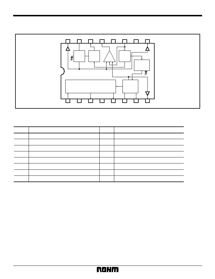
Block diagram
16
15
14
13
12
11
10
9
1
2
3
4
5
6
7
8
H.OSC
PHASE
COMP
6dB
AMP
V.SEPA
V.OSC
V.DRIVE
V.BLK
H.BLK
SYNC
SEPA
3
Video ICs
BA7149F
∑
Electrical characteristics (unless otherwise noted, Ta = 25∞C and Vcc = 5.0V)
Parameter
Symbol
Min.
Typ.
Max.
Unit
I
CC
31.0
42.0
55.0
mA
G
V
5.3
6.0
6.7
dB
D
RV
3.20
3.50
--
f
C
≠ 2.0
0.0
+ 2.0
dB
--
45
120
T
H ∑ BL
9.6
10.7
11.4
µ
s
T
V ∑ BL
870
970
1070
µ
s
f
H ∑ O
13.9
15.7
17.5
f
CAP
±
2.1
±
3.0
--
T
HP
10.2
11.1
12.0
µ
s
T
HPH
≠ 1.9
≠ 1.2
≠ 0.5
µ
s
V
HPL
0.5
1.1
1.7
V
f
V ∑ O
51.3
54.8
58.2
Hz
2.10
2.70
--
2.10
2.70
--
T
HVD
17.3
21.3
25.3
µ
s
T
HD
8.7
9.9
11.1
µ
s
T
VD
860
960
1060
µ
s
V
HV ∑ L
--
0.1
0.3
V
V
HV ∑ H
4.7
4.9
--
V
V
P-P
mV
P-P
V
P-P
V
P-P
kHz
kHz
V
syn ∑ Min.
V
VP ∑ Max.
V
VN ∑ Max.
Not designed for radiation resistance.
Operating current dissipation
Voltage gain
D range
Frequency characteristic
Minimum sync separation voltage
Horizontal blanking width
Vertical blanking width
Free-running frequency
Capture range
AFC output pulse width
AFC lock-in phase
Pulse voltage low
Free-running frequency
Pin 3 maximum output amplitude
Pin 5 maximum output amplitude
Phase difference
H
D
pulse width
V pulse width
Pulse voltage low
Pulse voltage high
VIDEO AMP
H
D
∑ V
D
Horizontal
Vertical
5
Video ICs
BA7149F
16pin
2pin
16pin
500
20k
12pin
20k
Fig.11
15pin
12pin
10k
15pin
2k
2k
2.8V
10k
10k
12k
V
+
Fig.10
∑
Circuit operation
Input signals
63.556
µ
H Pulse only
0.29V at 11pin
adj.at 11pin
4.7
µ
262.5H
16.683m
V Pulse only
H Pulse only
Pulse IH
Pulse IS
Pulse IV
IH
Fig.12
The video signal input to pin 11 is detected by the charg-
ing and discharging of an external capacitor. Sync sepa-
ration is done in the SYNC SEPA block. The H. SYNC
signal is sent to the H. OSC, and the V. SYNC signal is
sync-separated in the vertical sync pulse interval and sup-
plied to the V. OSC block.
The H. OSC block consists of a PLL that oscillates in sync
with the sync-separated H. SYNC signal, and outputs the
HD pulse and horizontal deflection pulse.
In the V. OSC block, a direct-control method is used with
the sync signal. To synchronize the vertical oscillator cir-
cuit, the inherent oscillation period of the oscillation circuit
is made slightly larger than the vertical sync signal period,
so that the sync signal always enters slightly early.
The oscillator output alone is not enough to ensure stable
operation for the vertical deflection output circuit, so it is
amplified by the V. DRIVE block.
The horizontal and vertical blanking signals generated in
the H. OSC and V. OSC blocks are used to erase the hor-
izontal retrace line from the video signal input to pin 11.
The signal is inverted and amplified by a 6dB inverting
amplifier and output as a negative-polarity video signal.