1
Multimedia ICs
NTSC color TV signal encoder
BA7230LS
The BA7230LS comprises an RGB signal matrix circuit, balanced modulator circuit (rectangular 2-phase modula-
tion), oscillator circuit (VCXO) for a 3.58MHz subcarrier synchronized with video input burst signals, luminosity and
color difference signal mixing circuit, and a high speed switch for selecting composite signals of video input and RGB
input. RGB signals, synch signals, BFP (burst flag pulses), PCP (pedestal clamp pulses) are input, and an NTSC
composite signal is output.
∑
Applications
Televisions (Teletext-capable), captain systems, video cameras, personal computers
∑
Features
1) Allows superimposition of video images (VIDEO IN)
and computer images (RGB IN).
2) During superimposition, the subcarrier locked onto
the video input burst signal RGB is modulated with
the RGB signals by the APC circuit, preventing
unnatural color disturbance due to switching.
3) Both the RGB and video input signals are pedestal-
clamped, maintaining a natural image even during
fluctuation in luminosity.
4) Using a half down pulse, the video signal can be
reduced by 5dB to darken the background and
make the superimposed RGB image easier to see.
5) Carrier leak is suppressible to less than 70mV
P-P
(V
OUT
= 2V
P-P
) without adjustment.
6) Can be adapted for analog RGB input.
7) Compact 24-pin SZIP package minimizes external
components.
∑
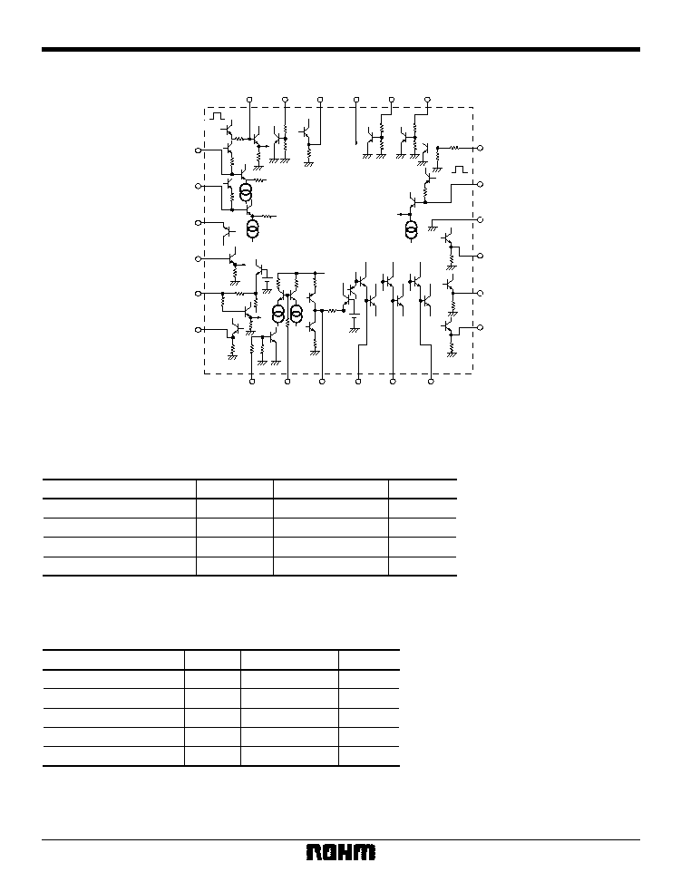
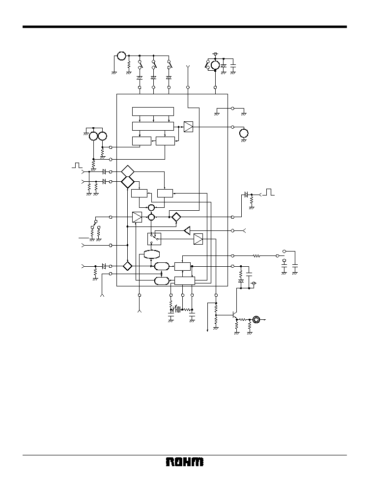
Block diagram
1
VIDEO OUT
3
Y IN
5
R-Y IN
7
V
C
9
APC PHASE
ADJUSTMENT
11
V
A
13
AR
15
AB
17
B-Y OUT
19
GND
21
PCP IN
23
Y
S
P IN
2
SYNC IN
BA7230LS
4
B-Y IN
6
PD
8
V
B
10
BURST LEVEL
ADJUSTMENT
12
BFP IN
14
AG
16
Y OUT
18
R-Y OUT
20
VIDEO IN
22
HDP IN
24
V
CC
V
CC
B - Y
R - Y
+
HD
MATRIX
PD
VCXO
MOD
MOD
+

3
Multimedia ICs
BA7230LS
∑
Electrical characteristics (unless otherwise noted, Ta = 25∞C, V
CC
= 5.0V)
Parameter
Symbol
Min.
Typ.
Max.
Conditions
Quiescent current
I
Q
--
38
54
mA
--
Video output level
V
OV
1.7
2.2
2.6
V
P-P
VIDEO IN = 1V
P-P
Half down level change
G
VH
≠ 3
≠ 5
≠ 7
dB
--
DC offset
V
OF
--
50
160
mV
P-P
VIDEO IN = 1V
P-P
Crosstalk
CT
--
≠ 46
≠ 40
dB
VIDEO IN = 1V
P-P
V
R-Y
0.3
0.42
0.55
V
P-P
V
B-Y
0.2
0.31
0.42
V
P-P
YOUT output level
V
Y
1.0
1.4
1.8
V
P-P
V
R
= V
G
= V
B
= 0.7V
P-P
Ys switching delay time
T
D
--
60
--
ns
--
--
SYNC output level
V
OS
0.4
0.65
0.9
V
P-P
Burst output level
V
OB
0.25
0.46
0.8
V
P-P
R
E
= 1.8k
Composite output level
V
OY
1.7
2.2
2.6
V
P-P
Y
IN
= 0.7V
P-P
G
R-Y
9
11
13
dB
G
B-Y
9
11
13
dB
G
R-B
--
--
2
dB
Difference between above gains
≠ 6
--
6
deg
--
≠ 6
--
6
deg
--
Carrier leak
L
SC
--
30
70
mV
P-P
V
OUT
= 2V
P-P
APC capture range
f
CAP
±
100
--
--
Hz
Carrier phase range
SC
±
30
±
45
--
deg
Superimposition
Video frequency characteristic
f
V
4.5
6
--
MHz
≠ 3dB when f = 100kHz
Video output DG
DG
--
±
3.5
--
%
VIDEO IN = 1V
P-P
Video output DP
DP
--
±
2.5
--
deg
VIDEO IN = 1V
P-P
Z
T
8
15
--
k
--
Input impedance (Ys)
Z
TY
3
7.5
--
k
--
V
T
0.9
2.0
2.8
V
--
Threshold level (Ys)
V
TY
0.5
1.1
1.8
V
--
Unit
ER-EY output level
EB-EY output level
R-Y modulation gain
B-Y modulation gain
(R-Y) / (B-Y) modulation gain differential
(R-Y) / (B-Y) orthogonal phase shift
(R - Y) ∑Burst orthogonal phase shift
Input impedance (SY, BF, PC, HD)
Threshold level (SY, BF, PC, HD)
V
R
= 0.7V
P-P
V
B
= 0.7V
P-P
R - Y
IN
= 0.3V
P-P
B - Y
IN
= 0.2V
P-P
Burst = 0.1V
P-P
, 2.8
µ
S
R
B