 | –≠–ª–µ–∫—Ç—Ä–æ–Ω–Ω—ã–π –∫–æ–º–ø–æ–Ω–µ–Ω—Ç: BA7242 | –°–∫–∞—á–∞—Ç—å:  PDF PDF  ZIP ZIP |
1
Multimedia ICs
Color TV signal encoder
BA7242F
The BA7242F is an IC which converts analog RGB signals to NTSC and PAL color TV signals. In addition to com-
posite output, luminance output, chrominance output, and analog RGB output are available. Each type of output is
equipped with an internal 75
driver.
∑
Applications
TV peripheral devices
∑
Features
1) Supports both NTSC and PAL systems.
2) Internal flip-flop circuit for PAL common mode
switching
3) Equipped with Y / C separated output pin.
4) Internal 75
driver
5) Supports subcarrier pulse for color input
∑
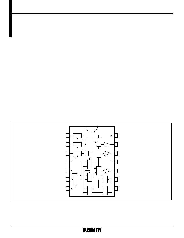
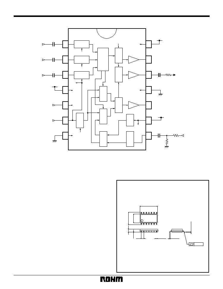
Block diagram
1
2
3
4
5
6
7
BIN
GIN
RIN
V
CC
1
SYNC
BFP
GND1
V
CC
2
Y
OUT
V
OUT
GND2
C
OUT
NT / PAL
SCIN
14
13
12
11
10
9
8
CLAMP
BFP
BFP
BFP
V
CC
SYNC
NT / PAL
BURST
FLAG
R-Y
MOD
F ∑ F
B-Y
MOD
CHROMA
GEN
Y / C
MIX
SYNC
MIX
SYNC
V
CC
GND
NT / PAL
MATRIX
PHASE
GEN
FILTER
GND
CLAMP
CLAMP
2
Multimedia ICs
BA7242F
∑
Absolute maximum ratings (Ta = 25∞C)
Parameter
Symbol
Limits
7
450
≠ 20 ~ + 70
≠ 55 ~ + 125
Unit
V
mW
∞
C
∞
C
V
CC
Pd
Topr
Tstg
Power supply voltage
Power dissipation
Operating temperature
Storage temperature
Reduced by 4.5mW for each increase in Ta of 1
∞
C over 25
∞
C.
(When mounted on a 70mm
◊
70mm
◊
1.6mm glass epoxy board.)
∑
Recommended operating conditions (Ta = 25∞C)
Parameter
Symbol
Limits
4.5 ~ 5.5
0 ~ 0.7
0 ~ 0.7
0 ~ 0.7
0.45 ~ 0.60
Unit
V
V
P≠P
V
P≠P
V
P≠P
V
P≠P
V
CC
RI
GI
BI
SC
Power supply voltage
RIN input level
GIN input level
BIN input level
SCIN input level
∑
Pin descriptions
Pin No.
1
Pin name
Function
BIN
Input for analog B signal. Operate with low impedance.
Input for analog G signal. Operate with low impedance.
Input for analog R signal. Operate with low impedance.
V
CC
for all except 75
driver.
GND for all except 75
driver.
3.58MHz or 4.43MHz pulse signal input.
Video signal output mode setting. HIGH level = NTSC, LOW level = PAL.
Chrominance signal output. Internal 75
driver.
GND for 75
driver.
Composite video signal output. Internal 75
driver.
Luminance signal output. Internal 75
driver.
V
CC
for 75
driver.
2
GIN
3
RIN
4
V
CC
1
5
SYNC
6
BFP
7
GND1
8
SCIN
9
NT / PAL
10
C
OUT
11
GND2
12
V
OUT
13
Y
OUT
14
V
CC
2
Input for composite SYNC signal. Outputs SYNC signal to VOUT and YOUT pins
when input is LOW.
Input for burst timing signal. Simultaneously performs the burst output and initiates
the pedestal clamp for the RIN, GIN, and BIN input signals when input is LOW.
3
Multimedia ICs
BA7242F
∑
Electrical characteristics (unless otherwise noted, Ta = 25∞C, V
CC
= 5V, SCIN = 3.579545MHz, NT / PAL = 5V)
Parameter
Symbol
Min.
23
0.63
0.19
0.37
Typ.
0.70
0.21
0.41
Max.
45
0.77
0.23
I
CC
L
L(R)
L(G)
Current consumption
Luminance level
Luminance level R
Luminance level G
Unit
mA
V
P-P
V
P-P
V
P-P
Conditions
RI
=
GI
=
BI
= 0.7V
P-P
RI
= 0.7V
P-P
2
GI
= 0.7V
P-P
2
BI
= 0.7V
P-P
2
0.07
0.08
0.45
L(B)
Luminance level B
V
P-P
0.27
0.30
0.09
S
R
S / L
Synchronization level
V
P-P
0.38
2.84
2.65
94
2.01
231
337
0.26
--
125
215
225
145
0.9
1.60
2.20
1.35
1.75
2.15
3.00
V
2.0
--
--
V
0.43
3.16
2.95
2.24
104
241
347
0.29
--
135
1.0
2.00
2.60
0.33
0.48
3.48
3.25
2.47
114
251
357
0.32
35
235
deg
1.1
2.40
R
R / BU
R
G / BU
R
B / BU
R
G
B
BU
CL
BU +
BU ≠
R
BU
V
YO
V
CO
V
VO
V
IH
V
IL
--
V
IH
--
V
IL
--
--
--
--
0.8
300
200
V
µ
A
µ
A
With 0V applied
With 5V applied
Synchronization /
luminance level ratio
Red / burst level ratio
Green / burst level ratio
Blue / burst level ratio
Red phase
Green phase
Blue phase
Burst level
--
--
--
--
deg
2
2
2
4
3
deg
deg
V
P-P
mV
P-P
deg
--
V
V
R
YO
=
YS
/
YL
RI
= 0.7V
P-P
2
GI
= 0.7V
P-P
2
BI
= 0.7V
P-P
2
NT / PAL = 0V
2
NT / PAL = 0V
2
NT / PAL = 0V
2
Carrier leak
PAL burst phase
PAL burst ratio
YOUT DC voltage
COUT DC voltage
VOUT DC Voltage
High level input voltage
SYNC, BFP, NT / PAL
Low level input voltage
SYNC, BFP, NT / PAL
Input current during high
SYNC, BFP, NT / PAL
Input current during low
SYNC, BFP, NT / PAL
34
YOUT
VOUT
COUT
VOUT
2 Guaranteed design with these parameters
3 Measured using a 3.58MHz BPF for 3.5
µ
s after the burst.
4 Measured using a 3.58MHz BPF.
Not designed for radiation resistance
4
Multimedia ICs
BA7242F
∑
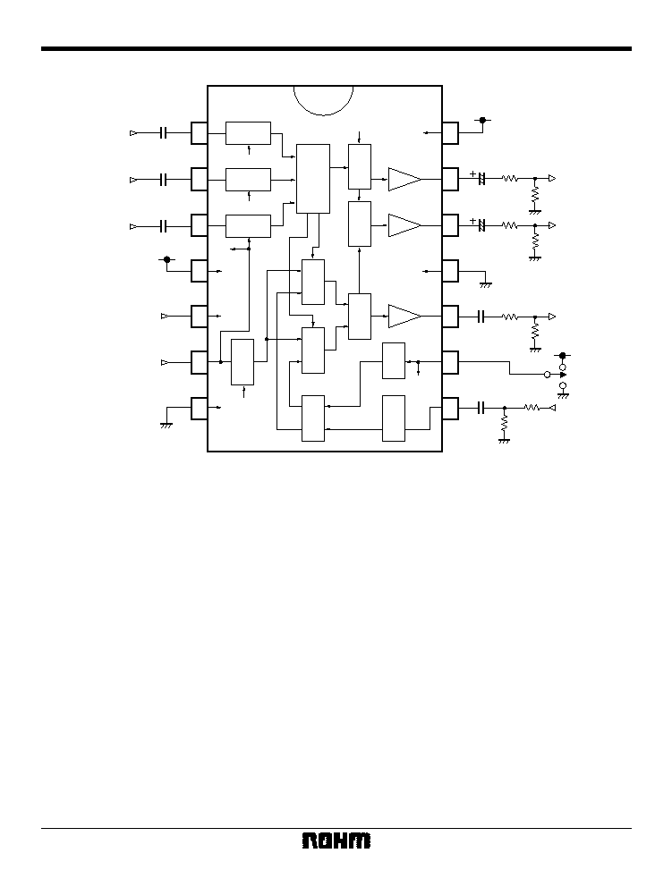
Measurement circuit
1
2
3
4
5
6
7
BIN input
GIN input
RIN input
V
CC
Composite SYNC
(BFP)
Burst flag pulse
YOUT
measurement point
Vcc
14
13
11
10
9
9
8
CLAMP
BFP
BFP
BFP
V
CC
SYNC
NT / PAL
BURST
FLAG
R-Y
MOD
F ∑ F
B-Y
MOD
CHROMA
GEN
Y / C
MIX
SYNC
MIX
SYNC
V
CC
GND
NT / PAL
MATRIX
PHASE
GEN
FILTER
GND
CLAMP
CLAMP
0.1
µ
0.1
µ
0.1
µ
V
CC
VOUT
measurement point
75
75
75
75
75
220
µ
220
µ
COUT
measurement point
75
0.47
µ
0.1
µ
560
4.7k
Color subcarrier
12
(1) The composite SYNC is input to the SYNCIN pin.
During Low level input, the SYNC signal is output to
the YOUT, VOUT, and SYNCOUT pins.
(2) The burst flag pulse is input to the BFPIN pin.
During Low level input, the burst signal is output to the
COUT and VOUT pins. For PAL, the phase inversion of
the chroma signal occurs according to this signal.
Furthermore, this signal also acts as the timing for the
pedestal clamp for the RIN, GIN, and BIN pins. By
using an external condenser for charging during Low
level input, the pedestal levels for the RIN, GIN, and
BIN pins are maintained at a uniform level.
(3) The NT / PAL pin is for selecting either NTSC or
PAL. For NTSC, this pin is connected to V
CC
and for
PAL, this pin is connected to GND.
(4) The SCIN pin is the color subcarrier input pin. Input
either a pulse wave or a sine wave of frequency
3.579545MHz for NTSC or of frequency 4.433619MHz
for PAL.
(5) The COUT pin is the output pin for the chroma sig-
nal, and the YOUT pin is the output pin for the lumi-
nance signal. This is compatible with the S pin because
the chroma signal and the luminance signal can be out-
put separately. Both pins have internal 75
drivers.
(6) The VOUT pin is the output pin for a color TV signal
and has an internal 75
driver.
∑
Operation description
5
Multimedia ICs
BA7242F
∑
Application example (When using NTSC color TV signal)
1
2
3
4
5
6
7
Analog B signal
Analog G signal
Analog R signal
V
CC
Composite SYNC
(BFP)
Burst flag pulse
V
CC
14
13
12
11
10
9
8
CLAMP
BFP
BFP
BFP
V
CC
SYNC
NT / PAL
BURST
FLAG
R-Y
MOD
F ∑ F
B-Y
MOD
CHROMA
GEN
Y / C
MIX
SYNC
MIX
SYNC
V
CC
GND
NT / PAL
MATRIX
PHASE
GEN
FILTER
GND
CLAMP
CLAMP
0.1
µ
0.1
µ
0.1
µ
V
CC
Color TV signal output
75
220
µ
0.1
µ
560
4.7k
Color subcarrier
+
∑
Operation notes
(1) Since analog RGB signals perform clamping at the
input pin, input them with a low impedance.
(2) Input a signal of duty 50% for the color subcarrier. If
the duty fluctuates, it will affect the chroma phase.
Furthermore, for the application example, a voltage-
dividing resistor is assumed for the CMOS input of 5V
P-P
.
For other input formats, regulate the SCIN pin for
0.5V
P-P
.
(3) Input the composite SYNC and burst flag pulse
according to the standard value. If the timing is off, the
TV receiver may not show any color. As well, set the
input level the same as the TTL level. The input imped-
ance is 8k
.
∑
External dimensions (Units: mm)
SOP14
0.4
±
0.1
1.27
1
14
8.7
±
0.2
7
8
4.4
±
0.2
6.2
±
0.3
0.11
1.5
±
0.1
0.15
0.15
±
0.1
0.3Min.