 | –≠–ª–µ–∫—Ç—Ä–æ–Ω–Ω—ã–π –∫–æ–º–ø–æ–Ω–µ–Ω—Ç: BA728N | –°–∫–∞—á–∞—Ç—å:  PDF PDF  ZIP ZIP |
1
Standard ICs
Dual operational amplifier
BA728 / BA728F / BA728N
The BA728, BA728F, and BA728N are ICs with two independently functioning operational amplifiers featuring inter-
nal phase compensation. These products offer a wide range of operating voltages, from 3 to 18V ( ± 1.5 to 9V) and
are high-performance operational amplifiers which can be driven from a single power supply within the in-phase
mode input range, including a negative power supply.
∑
Applications
Ground sensing small-signal amplifiers
Control amplifiers requiring high phase margin, such as motor drivers
Amplifiers operated on low voltages
Capacitive loaded amplifiers
∑
Features
1) Can be driven from a single power supply.
2) Low power.
3) Pin layout is the same as that of the general-
purpose 4558 operational amplifier.
4) When driven from a single power supply, the power
supply voltage ranges from 3 to 18V.
5) When driven from a dual power supply, the power
supply voltage ranges from ± 1.5 to ± 9V.
6) Output is protected against short-circuits.
7) Output block is operated as a class AB to mini-
mize crossover distortion.
8) Low input bias current of 10nA (typ.).
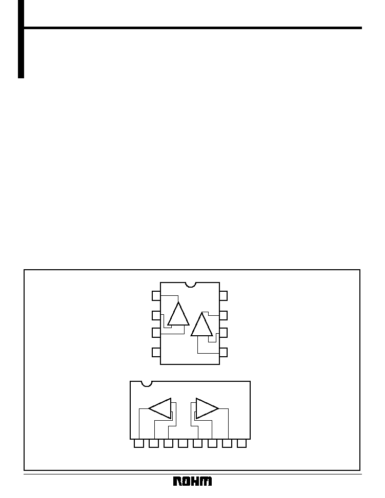
9) Each package contains two operational amplifiers.
10) Internal phase compensation provided.
∑
Block diagram
OUT1
≠
IN1
+
IN1
V
EE
V
CC
OUT2
≠
IN2
+
IN2
1
2
3
4
1
8
7
6
5
OUT1
2
≠
IN1
3
+
IN1
4
V
EE
5
+
IN2
6
≠
IN2
7
OUT2
8
V
CC
+
≠
+
+
≠
+
1ch
2ch
2ch
1ch
≠
≠
BA728 / BA728F
BA728N
2
Standard ICs
BA728 / BA728F / BA728N
∑
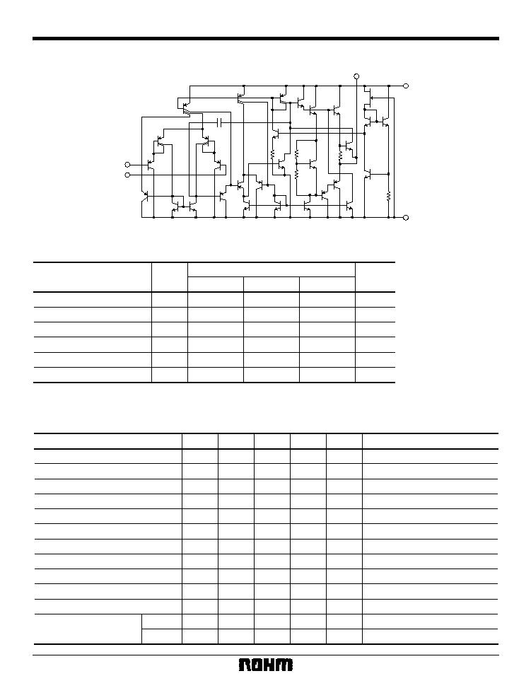
Internal circuit configuration
+
IN
≠
IN
Q
1
Q
4
Q
5
Q
2
Q
3
Q
6
Q
13
Q
16
Q
10
Q
11
Q
12
Q
14
Q
21
R
3
R
2
R
6
R
4
R
5
R
1
Q
20
Q
17
Q
15
Q
22
Q
23
Q
28
Q
25
Q
24
Q
19
Q
18
Q
27
Q
29
Q
26
Q
7
Q
8
Q
9
C
1
V
EE
V
CC
OUT
∑
Absolute maximum ratings (Ta = 25∞C)
Parameter
Symbol
Limits
Unit
BA728
BA728F
BA728N
V
CC
18 (
±
9)
18 (
±
9)
18 (
±
9)
V
Pd
800
550
550
mW
V
ID
V
CC
V
V
I
≠ 0.3 ~ + V
CC
V
Topr
≠ 20 ~ + 75
≠ 20 ~ + 75
≠ 20 ~ + 75
∞
C
Tstg
≠ 55 ~ + 125
≠ 55 ~ + 125
≠ 55 ~ + 125
∞
C
V
CC
V
CC
≠ 0.3 ~ + V
CC
≠ 0.3 ~ + V
CC
Power supply voltage
Power dissipation
Differential input voltage
Common-mode input voltage
Operating temperature
Storage temperature
Refer to Pd characteristics diagram.
The values for the BA728Fare those when it is mounted on a glass epoxy PCB (50mm
◊
50mm
◊
1.6mm).
∑
Electrical characteristics (unless otherwise noted, Ta = 25∞C, V
CC
= + 6V, V
EE
= - 6V)
Parameter
Symbol
Min.
Typ.
Max.
Conditions
V
IO
--
2
10
mV
I
IO
--
1
50
nA
I
B
--
10
250
nA
A
V
86
100
--
dB
R
L
2k
V
ICM
--
V
±
3.0
±
4.5
--
V
R
L
2k
CMRR
70
90
--
dB
PSRR
--
30
150
µ
V / V
--
0.7
--
V /
µ
S
--
0.7
--
MHz
CS
--
120
--
dB
source
Isource
--
20
--
mA
sink
Isink
--
10
--
mA
S. R.
f
T
Unit
A
V
= 1, R
L
= 2k
V
IN
+
= 1V, V
IN
≠
= 0V
V
IN
≠
= 1V, V
IN
+
= 0V
V
OM
4 ~ ≠ 6 4.5 ~ ≠ 6
Input offset voltage
Input offset current
Input bias current
High-amplitude voltage gain
Common-mode input voltage
Maximum output voltage
Common mode rejection ratio
Power supply voltage rejection ratio
Slew rate
Maximum frequency
Channel separation
Maximum output current
3
Standard ICs
BA728 / BA728F / BA728N
∑
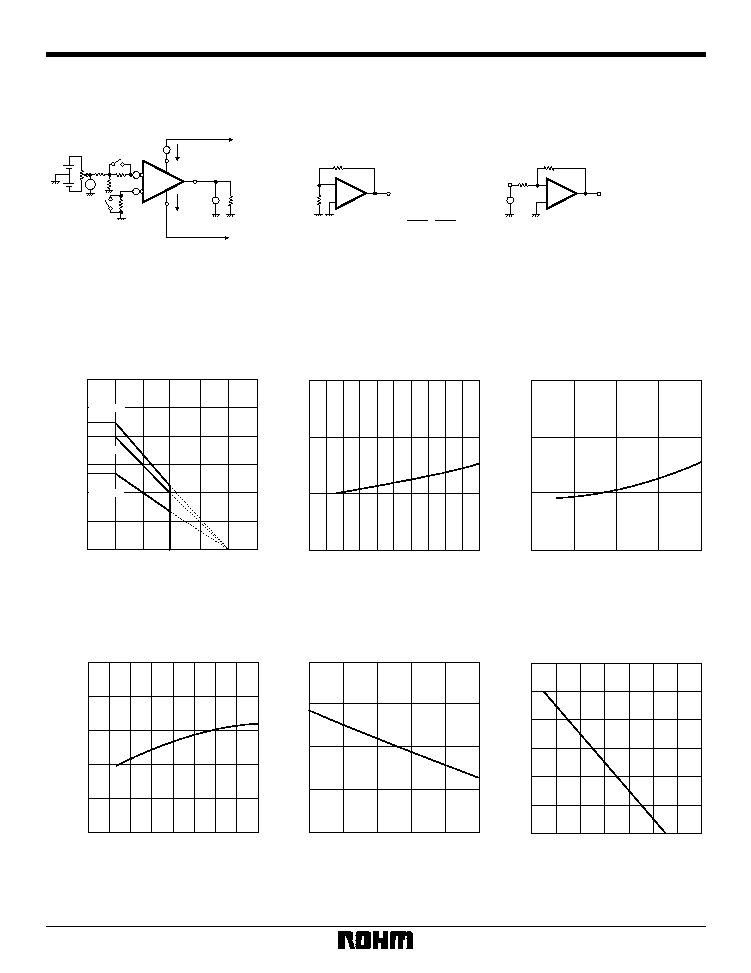
Measurement circuits
200
R
S
R
S
1
V
S
I
C
V
EE
V
CC
R
L
BA728
BA728F
BA728N
(per circuit)
50k
50
V
O
2
+
≠
1ch
=
≠ 200 log
1000
1
V
O
1
V
O
2
∑
Channel separation
Fig. 1 Channel separation measurement circuit
10k
10k
V
O
1
+
≠
2ch
~
(indicates individual channels
in the same package)
∑
Electrical characteristic curves
POWER DISSIPATION: Pd
(mW)
AMBIENT TEMPERATURE: Ta (
∞
C)
1200
1000
800
600
400
200
0
0
25
50
75
100
125
150
BA728
BA728N
Fig.2 Power dissipation vs. ambient
temperature
BA728F
3
2
1
0
0
10
20
QUIESCENT CURRENT: l
Q
(mA)
POWER SUPPLY VOLTAGE: V +
(V)
Fig.3 Quiescent current vs.
power supply voltage
10
20
30
0
10
20
INPUT BIAS CURRENT: l
d
(nA)
POWER SUPPLY VOLTAGE: V +
(V)
Fig.4 Input bias current vs.
power supply voltage
160
10
20
0
120
80
OPEN LOOP VOLTAGE GAIN: A
V
(dB)
POWER SUPPLY VOLTAGE: V +
(V)
Fig.5 Open loop voltage gain vs.
power supply voltage
40
30
20
10
0
≠
20
0
20
40
80
60
OUTPUT CURRENT: l
O
(mA)
AMBIENT TEMPERATURE: Ta (
∞
C)
Fig.6 Current control characteristics
120
100
80
60
40
20
0
10M
1M
100k
10k
1k
100
10
1
OPEN LOOP VOLTAGE GAIN: A
V
(dB)
FREQUENCY: f
(Hz)
Fig.7 Open loop voltage gain vs.
frequency
20
15
100k
10k
1k
100
1M
10
5
0
FREQUENCY: f (Hz)
MAXIMUM OUTPUT VOLTAGE: V
OM
(W)
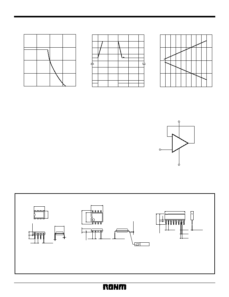
Fig.8 Maximum output voltage vs.
frequency
4
2
0
1
2
3
1
3
0
20
40
30
10
0
V
IN
(V)
INPUT VOLTAGE
V
OUT
(V)
OUTPUT VOLTAGE
TIME (
µ
s)
Fig.9 Output response characteristics
10
5
0
≠ 5
≠ 10
0
±
5
±
10
MAXIMUM OUTPUT VOLTAGE: V
OM
(V)
POWER SUPPLY VOLTAGE: V
±
(V)
Fig.10 Maximum output voltage vs.
power supply voltage
(1)Unused circuit connections
If there are any circuits which are not being used, we
recommend making connections as shown in Figure
11, with the non-inverted input pin connected to the
potential within the in-phase input voltage range (V
ICM
).
4
Standard ICs
BA728 / BA728F / BA728N
∑
Operation notes
≠
+
V
EE
V
CC
To potential
in V
ICM
Fig.11 Unused circuit connections
∑
External dimensions (Units: mm)
DIP8
SOP8
SIP8
BA728
BA728F
BA728N
0.5
±
0.1
3.2
±
0.2
3.4
±
0.3
8
5
1
4
9.3
±
0.3
6.5
±
0.3
0.3
±
0.1
0.51Min.
2.54
0
∞
~ 15
∞
7.62
0.4
±
0.1
1.27
0.15
0.3Min.
0.15
±
0.1
0.11
6.2
±
0.3
4.4
±
0.2
5.0
±
0.2
8
5
4
1
1.5
±
0.1
10.5
±
0.5
1
8
2.54
3.5
±
0.5
1.3
0.8
0.6
0.3
±
0.1
2.8
±
0.2
19.3
±
0.2
1.2
5.8
±
0.2
∑
Electrical characteristic curve