 | –≠–ª–µ–∫—Ç—Ä–æ–Ω–Ω—ã–π –∫–æ–º–ø–æ–Ω–µ–Ω—Ç: BA7602 | –°–∫–∞—á–∞—Ç—å:  PDF PDF  ZIP ZIP |
1
Multimedia ICs
Video signal switcher
BA7602 / BA7602F
The BA7602 and BA7602F are switching ICs developed for use in VCRs. Each contains three two-channel analog
multiplexers. They feature a large dynamic range, and wide operating frequency range, and are suitable for switching
audio and video signals.
∑
Applications
Video cassette recorders and televisions
∑
Features
1) Three 2-input / 1-output switches.
2) 5V power supply.
3) Low power consumption (70mW Typ.).
4) Excellent frequency characteristics
(10MHz, 0dB Typ.).
5) Wide dynamic range (3.1V
P-P
Typ.).
6) High input impedance (20k
Typ.).
7) Fast switching speed (50ns Typ.).
∑
Absolute maximum ratings (Ta = 25∞C)
Parameter
Symbol
Unit
V
CC
9
V
mV
Topr
∞
C
Tstg
≠ 55 ~ + 125
∞
C
500
≠ 40 ~ + 85
Limits
Pd
Power supply voltage
Power dissipation
Operating temperature
Storage temperature
Reduced by 5.0mW for each increase in Ta of 1
∞
C over 25
∞
C.
∑
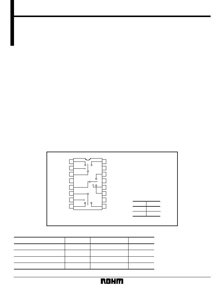
Block diagram
1
IN2a
2
CTLa
3
OUTa
4
GND
5
OUTb
6
OUTc
7
CTLc
8
IN2c
16 IN1a
15 GND
14 IN2b
13 V
CC
12 CTLb
11 IN1b
10 GND
9
IN1c
Sa
Sb
Sc
CTL
Output
L
IN2
H
IN1
2
Multimedia ICs
BA7602 / BA7602F
∑
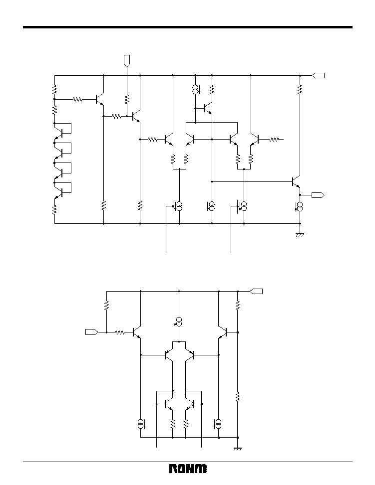
Equivalent circuits
Sa, Sb, Sc
R3
8.4k
R4
200
R6
20k
R5
33k
R8
25k
I1
0.6mA
I2
0.3mA
I3
0.5mA
I4
0.6mA
I5
1mA
R7
100
R10
100
R11
100
R13
100
R14
100
R9
200
R12
200
R16
200
R15
200
R2
9.4k
R1
1k
Q4
Q5
Q6
Q7
Q8
Q10 Q11
Q12
Q9
Q3
Q2
Q1
OUT
V
CC
IN
R3
400
R4
400
R5
25k
R2
200
Q3
2
2
Q1
Q5
Q6
Q2
Q4
CTL
R6
25k
R1
50k
V
CC
I2
0.6mA
I1
0.25mA
I3
0.06mA
CTL
3
Multimedia ICs
BA7602 / BA7602F
∑
Electrical characteristics (unless otherwise noted, Ta = 25∞C, V
CC
= 5.0V)
Parameter
Symbol
Min.
Typ.
Max.
Unit
Conditions
V
CC
4.5
5.0
5.5
V
--
I
CC
--
14.0
20.5
mA
--
2.8
3.1
--
V
P-P
G
V
≠ 0.5
0
C
T
--
≠ 65
--
G
f
≠ 3
0
dB
Z
IN
14
20
26
k
--
V
TH
20
2.5
3.0
V
--
dB
dB
f = 1kHz, THD = 0.5%
f = 1MHz, V
IN
= 1V
P-P
f = 4.43MHz, V
IN
= 1V
P-P
10MHz / 1MHz, V
IN
= 1V
P-P
0.5
1
V
om
Operating voltage
Supply current
Maximum output level
Voltage gain
Interchannel crosstalk
Frequency characteristic
Input impedance
CTL pin switch level
Note: Refer to the measurement circuit given in Fig. 1.
∑
Reference data
Pin DC voltages (reference values)
Pin No.
DC voltage
DC voltage
Pin No.
1
3.27
9
3.27
2
4.91
10
0
3
1.84
11
3.27
4
0
12
4.91
5
1.84
13
5.00
6
1.84
14
3.27
7
4.91
15
0
8
3.27
16
3.27
Units: Vdc
Parameter
--
20k
--
--
30
--
Min.
Typ.
Max.
Unit
The input coupling capacitor values should be 0.1
µ
F to 1
µ
F.
Input impedance (no clamp)
Output impedance
Electrical characteristics
4
Multimedia ICs
BA7602 / BA7602F
∑
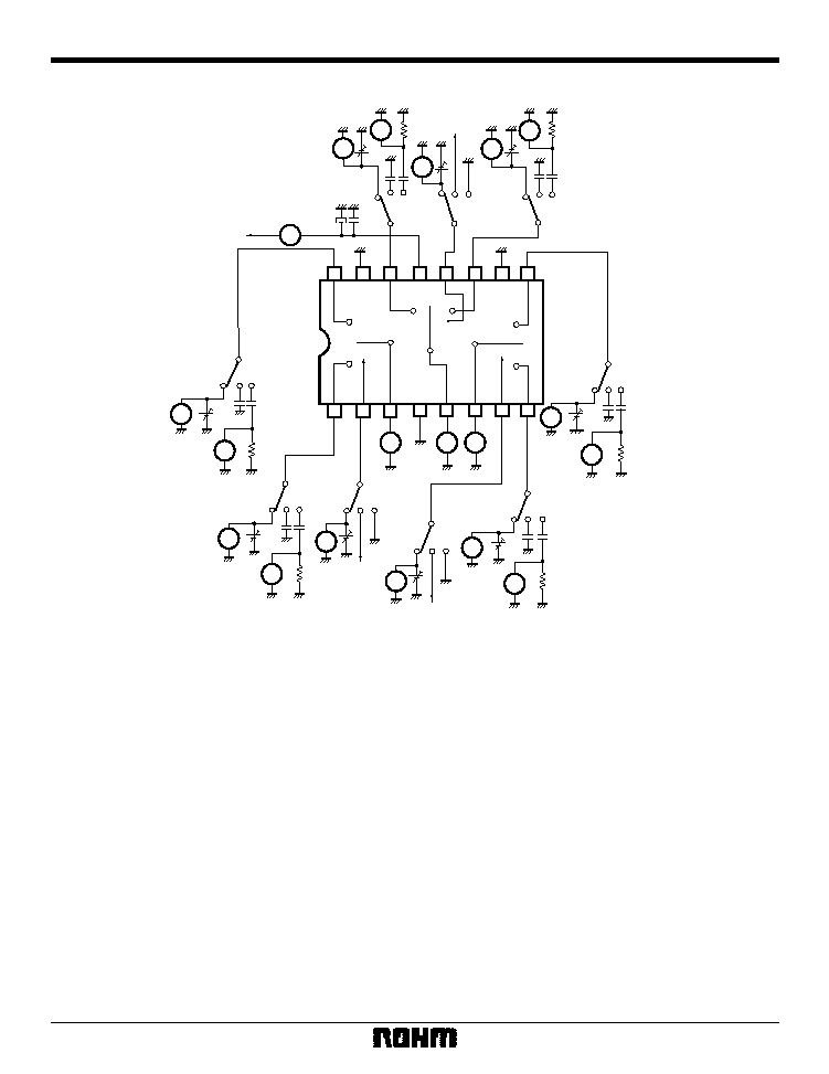
Measurement circuit
9
10
11
12
13
14
15
16
8
7
6
5
4
3
2
1
V
~
V
V
V
CC
V
CC
S
2b
S
3b
S
Ib
47 / 16
223
OSC
V
CC
V
OUTa
V
OUTb
V
OUTc
V
CC
OSC
OSC
OSC
50
50
1
1
2
2
3
3
1
2 3
105
105
105
S
1C
S
2C
S
3C
S
3a
S
2a
S
ia
50
50
50
50
105
105
105
105
105
105
OSC
105
105
1
2 3
1 2
3
1
2
3
1
1
2 3
2 3
1
2
3
105
V
V
~
~
~
V
V
V
V
V
V
A
~
~
V
Fig.1
5
Multimedia ICs
BA7602 / BA7602F
S
1a
S
2a
S
3a
S
1b
S
2b
S
3b
S
1C
S
2C
S
3C
I
CC
2
2
2
2
2
2
2
2
2
I
N1a
I
N2a
I
N1b
I
N2b
I
N1c
I
N2c
3
2
2
2
2
2
2
3
2
2
2
2
2
3
2
2
2
2
2
2
3
2
2
2
2
2
2
3
2
2
2
2
2
3
2
2
2
2
2
2
3
2
2
2
2
2
2
3
2
2
2
2
2
3
I
N1a
I
N2a
I
N1b
I
N2b
I
N1c
I
N2c
G
V
G
V
G
V
G
V
G
V
G
V
3
2
2
2
2
2
2
3
2
2
2
2
2
3
2
2
2
2
2
2
3
2
2
2
2
2
2
3
2
2
2
2
2
3
2
2
2
2
2
2
3
2
2
2
2
2
2
3
2
2
2
2
2
3
I
N1a
I
N2a
I
N1b
I
N2b
I
N1c
I
N2c
C
T
C
T
C
T
C
T
C
T
C
T
2
3
2
2
2
2
3
2
2
2
2
2
2
3
2
2
2
2
2
2
2
3
2
2
2
2
3
2
2
2
2
2
2
3
2
2
2
2
2
2
2
3
2
2
2
2
3
2
2
2
2
2
2
3
I
N1a
I
N2a
I
N1b
I
N2b
I
N1c
I
N2c
G
f
G
f
G
f
G
f
G
f
G
f
3
2
2
2
2
2
2
3
2
2
2
2
2
3
2
2
2
2
2
2
3
2
2
2
2
2
2
3
2
2
2
2
2
3
2
2
2
2
2
2
3
2
2
2
2
2
2
3
2
2
2
2
2
3
CTLa
CTLb
CTLc
V
TH
V
TH
V
TH
3
2
2
2
2
2
1
2
2
2
3
2
2
2
2
2
1
2
2
2
3
2
2
2
2
2
1
I
N1a
I
N2a
I
N1b
I
N2b
I
N1c
I
N2c
Z
IN
Z
IN
Z
IN
Z
IN
Z
IN
Z
IN
1
2
2
2
2
2
2
1
2
2
2
2
2
3
2
2
2
2
2
2
1
2
2
2
2
2
2
1
2
2
2
2
2
3
2
2
2
2
2
2
1
2
2
2
2
2
2
1
2
2
2
2
2
3
V
Om
V
Om
V
Om
V
Om
V
Om
V
Om
f = 1kHz
THD = 0.5%
f = 1kHz
V = 1V
P-P
f = 4.43MHz
V = 1V
PP
f = 10M / f = 1M
V = 1V
PP
Note 5
Note 6
Note 1
Note 2
Note 3
Note 4
Parameter
Symbol
Switch settings
Measurement
method
Current dissipation
Maximum
output level
Voltage gain
Interchannel
crosstalk
Frequency
characteristic
CTL pin
switching level
Input
impedance
Note 1: Connect a distortion meter to the output, and input a f = 1kHz sine wave. Adjust the output level until the output distortion is 0.5%.
This output voltage at this time is the maximum output level V
om
(V
P-P
).
Note 2: Input a 1V
P-P
, 1MHz sine wave. The voltage gain is given by G
V
= 20 log (V
OUT
/ V
IN
).
Note 3: Input a 1V
P-P
, 4.43MHz sine wave. The interchannel crosstalk is given by C
T
= 20 log (V
OUT
/ V
IN
).
Note 4: Input 1V
P-P
, 1MHz and 10MHz sine waves. The frequency characteristic is given by G
f
= 20 log (V
OUT
(f = 10MHz) / V
OUT
(f = 1MHz)).
Note 5: Input a 1V
P-P
, 1MHz sine wave. Reduce the CTL pin voltage from V
CC
.
The CTL pin switching level (V
TH
) is the CTL pin voltage at which the Vout level drops below 20mV
P-P
.
Note 6: Measure the input pin voltage V
IN50
when a current of DC50
µ
A is flowing into the input pin. Measure the input pin open-circuit voltage.
The input impedance is given by Z = (V
IN50
- V
IN0
) / 50
◊
10
-6
[
].
∑
Measurment conditions