1
Multimedia ICs
Video signal switcher
BA7604N
The BA7604N is a switching IC developed for use in VCRs. It has two-channel analog multiplexers, and features
wide dynamic range, and wide operating frequency range, and is suitable for switching audio and video signals.
∑
Applications
VCRs and TVs
∑
Features
1) Two 2-input / 1-output switches.
2) 5V power supply.
3) Low power consumption (42mW Typ.).
4) Excellent frequency characteristics
(10MHz, 0dB, Typ.).
5) Wide dynamic range (3.0V
P-P
Typ.).
6) High input impedance (20k
Typ.).
7) Fast switching speed (50ns Typ.).
∑
Absolute maximum ratings (Ta = 25∞C)
Parameter
Symbol
Limits
Unit
9
V
mW
∞
C
∞
C
500
V
CC
Topr
Pd
Tstg
≠ 40 ~ + 85
≠ 55 ~ + 125
Power supply voltage
Power dissipation
Operating temperature
Storage temperature
Reduced by 5.0mW for each increase in Ta of 1
∞
C over 25
∞
C.
∑
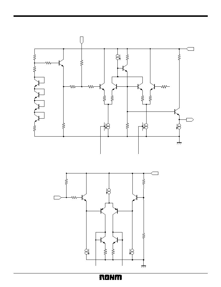
Block diagram
S
a
S
b
1
2
3
4
5
6
7
8
9
10
IN1a
V
CC
IN2a
CTLa
OUTa
OUTb
CTLb
IN2b
GND
IN1b
L
IN2
H
IN1
CTL
Output
S
a
, S
b
: Non-clamped
3
Multimedia ICs
BA7604N
∑
Electrical characteristics (unless otherwise noted, Ta = 25∞C and V
CC
= 5.0V)
Parameter
Symbol
Typ.
Max.
Unit
Conditions
V
CC
4.5
5.0
5.5
V
--
I
CC
--
8.4
13.0
mA
--
2.7
3.0
--
f = 1kHz, THD = 0.5%
G
V
≠ 0.5
0
dB
C
T
--
≠ 65
--
dB
≠ 3
0
dB
THD
--
0.007
--
%
V
TH
2.0
2.5
3.0
V
--
14
20
26
k
--
Z
IN
G
f
V
om
f = 1MHz, V
IN
= 1V
P-P
f = 4.43MHz, V
IN
= 1V
P-P
f = 1MHz, V
IN
= 1V
P-P
10MHz / 1MHz, V
IN
= 1V
P-P
0.5
1
V
P-P
Min.
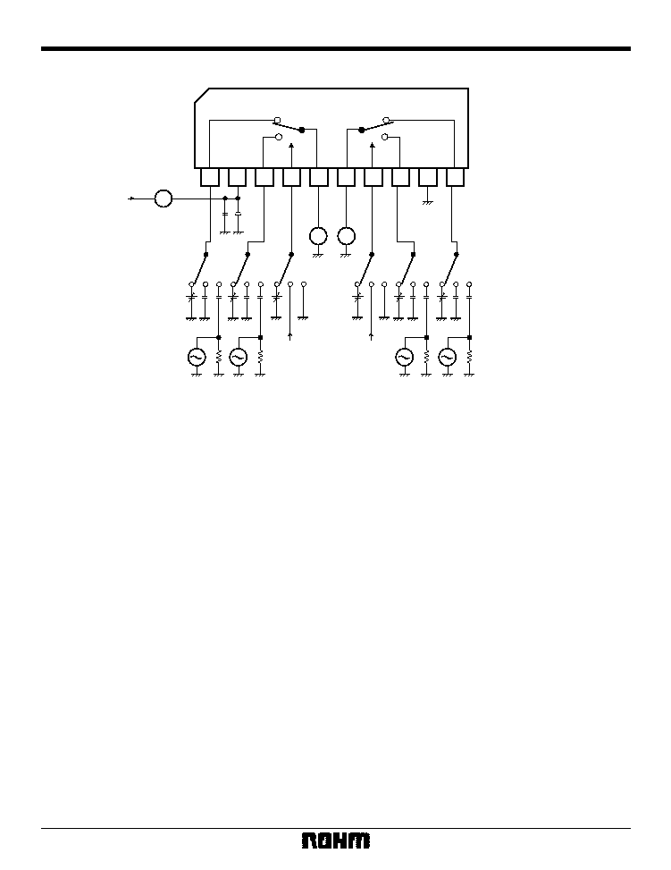
Note: Refer to the measurement circuit given in Fig. 1.
Operating voltage
Supply current
Maximum output level
Voltage gain
Interchannel crosstalk
Frequency characteristic
Total-harmonic distortion
CTL pin switch level
Input impedance
∑
Reference data
Pin DC voltages (reference values)
1
2.48
9
0
2
5.00
10
2.48
3
2.48
4
4.91
5
1.76
6
1.76
7
4.91
8
2.48
Pin No.
DC voltage
DC voltage
Pin No.
Units: Vdc
Electrical characteristics
Parameter
--
20k
--
--
30
--
Min.
Typ.
Max.
Unit
Input impedance (no clamp)
Output impedance
The input coupling capacitor values should be 0.1
µ
F to 1
µ
F.

5
Multimedia ICs
BA7604N
S
1a
S
2a
S
3a
S
1b
S
2b
S
3b
I
CC
2
2
2
2
2
2
I
N1a
I
N2a
I
N1b
I
N2b
V
om
V
om
V
om
V
om
3
2
2
2
2
3
2
2
2
3
2
2
2
2
3
2
2
2
2
3
2
2
2
3
I
N1a
I
N2a
I
N1b
I
N2b
G
V
G
V
G
V
G
V
3
2
2
2
2
3
2
2
2
3
2
2
2
2
3
2
2
2
2
3
2
2
2
3
I
N1a
I
N2a
I
N1b
I
N2b
2
3
2
2
3
2
2
2
2
3
2
2
2
2
2
3
2
2
3
2
2
2
2
3
I
N1a
I
N2a
I
N1b
I
N2b
G
f
G
f
G
f
G
f
3
2
2
2
2
3
2
2
2
3
2
2
2
2
3
2
2
2
2
3
2
2
2
3
CTLa
CTLb
V
TH
V
TH
3
2
2
2
1
2
2
3
2
2
2
1
I
N1a
I
N2a
I
N1b
I
N2b
THD
THD
THD
THD
3
2
2
2
2
3
2
2
2
3
2
2
2
2
3
2
2
2
2
3
2
2
2
3
I
N1a
I
N2a
I
N1b
I
N2b
Z
IN
Z
IN
Z
IN
Z
IN
1
2
2
2
2
1
2
2
2
3
2
2
2
2
1
2
2
2
2
1
2
2
2
3
C
T
C
T
C
T
C
T
Note 1
Ammeter
Note 2
Note 3
Note 4
Note 5
Note 6
Note 7
Parameter
Symbol
Switch settings
Measurement
method
Current dissipation
Maximum
output
level
Voltage
gain
Interchannel
crosstalk
Frequency
character-
istic
CTL pin
switching level
Total-
harmonic
distortion
Input
impedance
Note 1: Connect a distortion meter to the output, and input a f = 1kHz sine wave. Adjust the output level until the output
distortion is 0.5%. This output voltage at this time is the maximum output level Vom (V
P-P
).
Note 2: Input a 1V
P-P
, 1MHz sine wave. The voltage gain is given by G
V
= 20 log (V
OUT
/ V
IN
).
Note 3: Input a 1V
P-P
, 4.43MHz sine wave. The interchannel crosstalk is given by C
T
= 20 log (V
OUT
/ V
IN
).
Note 4: Input 1V
P-P
, 1MHz and 10MHz sine waves. The frequency characteristic is given by G
f
= 20 log (V
OUT
(f =
10MHz) / V
OUT
(f = 1MHz)).
Note 5: Input a 1V
P-P
, 1MHz sine wave. Reduce the CTL pin voltage from V
CC
. The CTL pin switching level (V
TH
) is the
CTL pin voltage at which the V
OUT
level drops below 20mV
P-P
.
Note 6: Input a 1V
P-P
, 1kHz sine wave and measure the total-harmonic distortion of the output using a total-harmonic dis-
tortion meter.
Note 7: Measure the input pin voltage V
IN50
when a current of DC50
µ
A is flowing into the input pin. Measure the input
pin open-circuit voltage. The input impedance is given by Z = (V
IN50
- V
IN0
) / 50
◊
10
-6
[
].
∑
Measurement conditions