1) Three 2-input / 1-output switches (one with sync-
clamped inputs, the other two non-clamped).
2) 5V power supply.
3) Low power consumption (62.5mW Typ.).
4) Excellent frequency characteristics
(10MHz, 0dB Typ.).
5) Wide dynamic range (clamped input: 2.9V
P-P
Typ.,
non-clamped input: 3.0V
P-P
, Typ.).
6) Fast switching speed (50ns Typ.).
1
Multimedia ICs
Video signal switcher
BA7609 / BA7609F
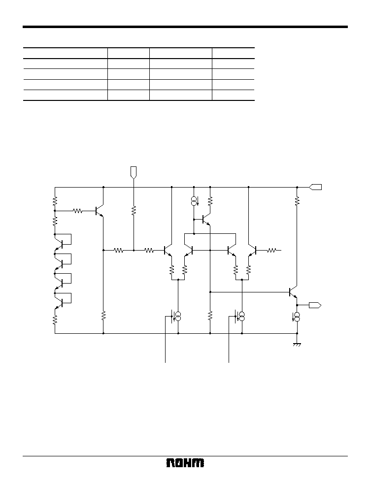
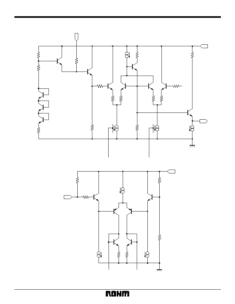
The BA7609 and BA7609F are switching ICs developed for use in VCRs. Each contains three two-channel analog
multiplexers. As one of the switches has sync-tip clamp inputs and the other two have non-clamped inputs these ICs
are ideal for switching audio, video and chroma signals.
∑
Applications
Video cassette recorders and televisions
∑
Features
∑
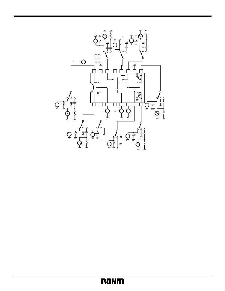
Block diagram
1
IN2a
2
CTLa
3
OUTa
4
GND
5
OUTb
6
OUTc
7
CTLc
8
IN2c
16
IN1a
15
GND
14
IN2b
13
V
CC
S
a
S
b
12
CTLb
11
IN1b
10
GND
9
IN1c
S
C
CTL
L
IN2
H
IN1
Output
S
a
, S
b
: non-clamped input
S
c
: clamped input
4
Multimedia ICs
BA7609 / BA7609F
∑
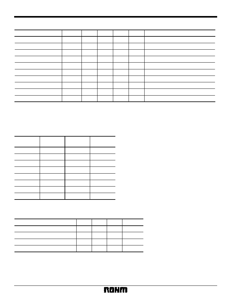
Electrical characteristics (unless otherwise noted, Ta = 25∞C and V
CC
= 5V)
Parameter
Symbol
Min.
Typ.
Max.
Unit
Conditions
V
CC
4.5
5.0
5.5
V
--
I
CC
--
12.5
20.0
mA
--
V
om
2.6
2.9
--
V
P-P
V
om
2.7
3.0
--
V
P-P
G
V
≠ 0.5
0
dB
--
≠ 65
--
dB
G
f
≠ 3
0
dB
Z
IN
14
20
26
k
THD
--
0.007
--
%
V
TH
2.0
2.5
3.0
V
--
C
T
10MHz / 1MHz, V
IN
= 1V
P-P
f = 1MHz, V
IN
= 1V
P-P
f = 4.43MHz, V
IN
= 1V
P-P
0.5
1
non-clamped input
f = 1kHz, 1V
P-P
non-clamped input
f = 1kHz, THD = 0.5% non-clamped input
f = 1kHz, THD = 0.5% clamped input
Operating voltage
Supply current
Maximum output level 1
Maximum output level 2
Voltage gain
Interchannel crosstalk
Frequency characteristic
Input impedance
Total-harmonic distortion
CTL pin switch level
Note: Refer to the measurement circuit given in Fig. 1.
∑
Reference data
Pin DC voltages (reference values)
1
2.48
9
2.05
2
4.91
10
0
3
1.76
11
2.48
4
0
12
4.91
5
1.76
13
5.00
6
0.65
14
2.48
7
4.91
15
0
8
2.05
16
2.48
Pin No.
DC voltage
DC voltage
Pin No.
Units: Vdc
Electrical characteristics
Parameter
0.49
0.65
0.80
Vdc
--
20k
--
--
1.7M
--
--
30
--
Min.
Typ.
Max.
Unit
The input coupling capacitor values should be 0.1
µ
F to 1
µ
F.
Sync tip clamp level
Input impedance (no clamp)
Input impedance (with clamp)
Output impedance