 | –≠–ª–µ–∫—Ç—Ä–æ–Ω–Ω—ã–π –∫–æ–º–ø–æ–Ω–µ–Ω—Ç: BA7649AF | –°–∫–∞—á–∞—Ç—å:  PDF PDF  ZIP ZIP |
1
Multimedia ICs
Video signal switcher
BA7649A / BA7649AF
The BA7649A and BA7649AF are five-channel analog multiplexers (the IN5 pin can be used a mute input) designed
for use in video cassette recorders. They feature large dynamic range, and wide operating frequency range, and
have sync-tip inputs which are ideal for switching video signals.
∑
Applications
Video cassette recorders and televisions
∑
Features
1) 5-input / 1-output switches.
2) Built-in mute (the IN5 pin can be use a mute input).
3) Sync-tip clamp inputs.
4) Wide operating supply voltage range
(4.5V to 13.0V).
5) Low power consumption (48mW Typ.).
6) Excellent frequency characteristics
(10MHz, 0dB Typ.).
7) Wide dynamic range (3.5V
P-P
Typ.).
8) Low interchannel crosstalk
( ≠ 65dB Typ., f = 4.43MHz).
9) DIP / SOP 14 pin package.
∑
Absolute maximum ratings (Ta = 25∞C)
BA7649A
Parameter
Symbol
Unit
V
CC
13.5
V
1100
mW
∞
C
∞
C
≠ 25 ~ + 75
≠ 55 ~ + 125
Topr
Tstg
Pd
Limits
Reduced by 11.0mW for each increase in Ta of 1
∞
C over 25
∞
C.
Power supply voltage
Allowable current
Operating temperature
Storage temperature
BA7649AF
Parameter
Symbol
Unit
V
CC
13.5
V
450
mW
∞
C
∞
C
≠ 25 ~ + 75
≠ 55 ~ + 125
Limits
Pd
Topr
Tstg
Power supply voltage
Allowable current
Operating temperature
Storage temperature
Reduced by 4.5mW for each increase in Ta of 1
∞
C over 25
∞
C when mounted on a 50mm
◊
50mm PCB board.
2
Multimedia ICs
BA7649A / BA7649AF
∑
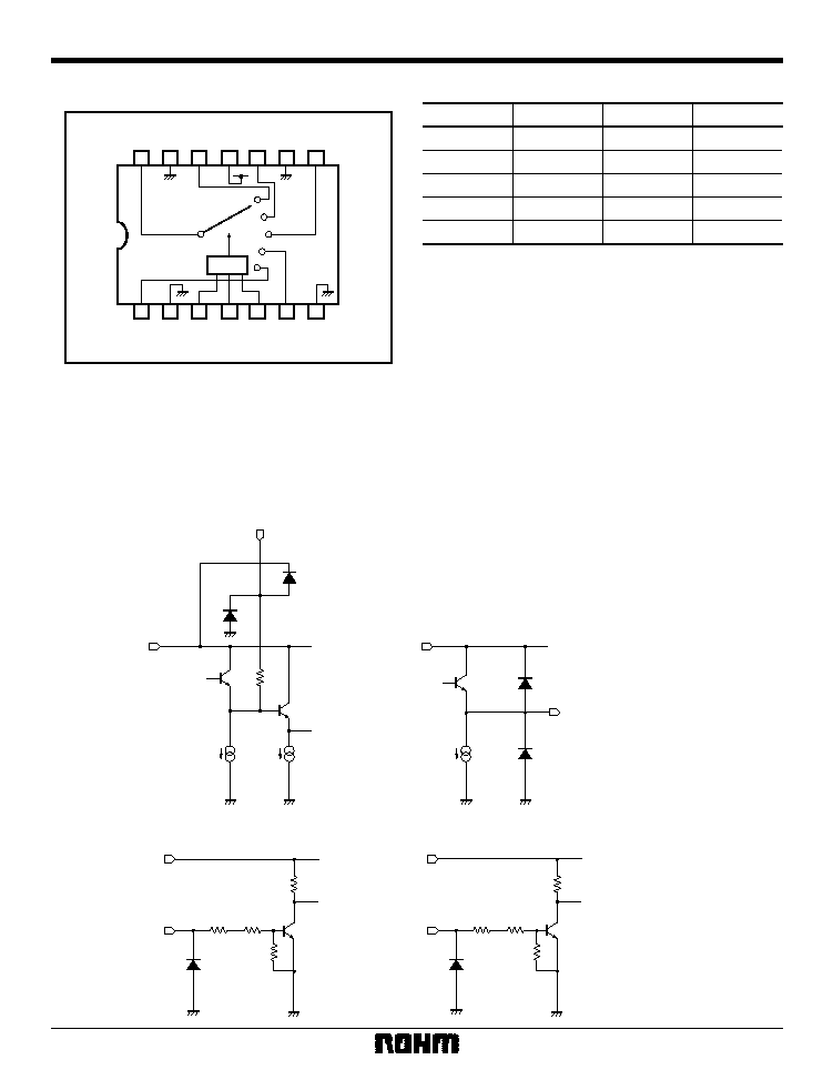
Equivalent circuits
0.8
µ
A
100
µ
A
Vcc
IN
D2
Q1
Q2
R2
100
D1
Input clamp voltage 2.1V (V
CC
= 5V, Typ.)
Input bias current 1
µ
A [Typ.]
Input impedance over 1M
2mA
Vcc
Q1
D1
OUT
D2
Output impedance 20
[Typ.]
Output DC voltage 0.55V (V
CC
= 5V, Typ.)
OUTPUT
CLAMP INPUT
100
50k
20k
34k
Vcc
CTLA / B
R4
R1
D2
R2
R3
Q3
CTLA / CTLB
100
45k
30k
29k
Vcc
CTLC
R4
R1
D2
R2
R3
Q3
CTLC
∑
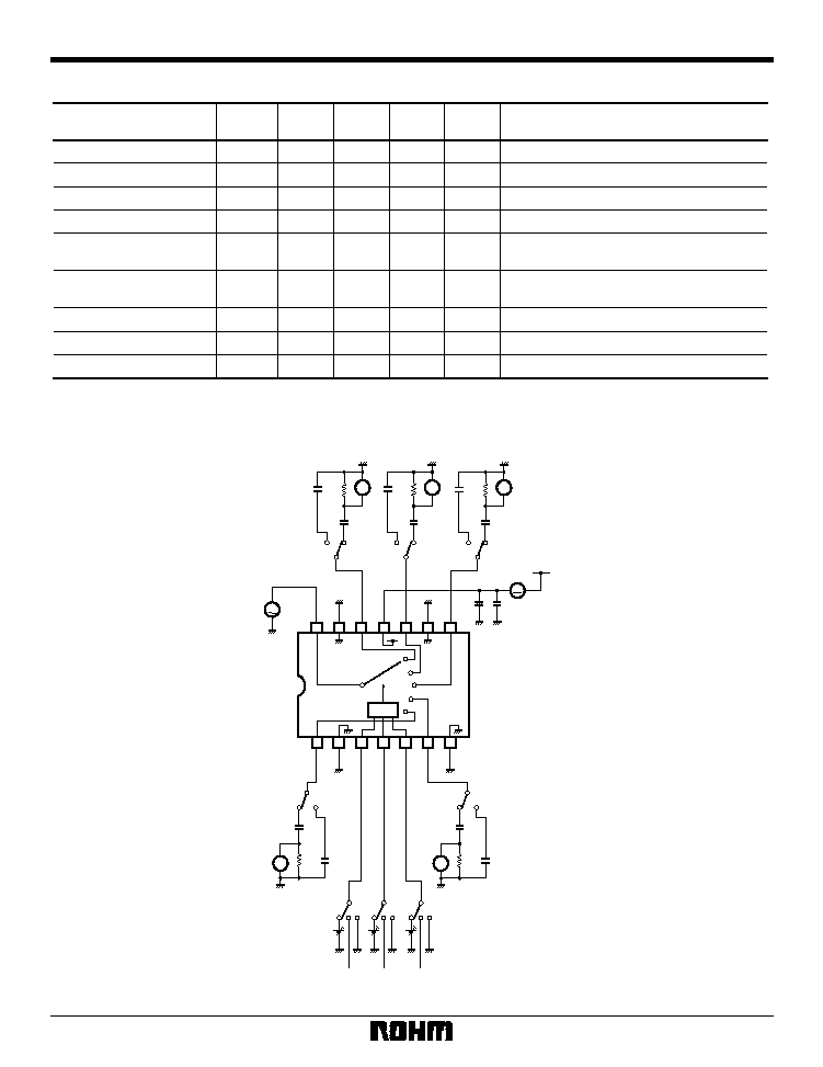
Block diagram
1
IN1
2
GND
3
CTL A
4
CTL B
5
CTL C
6
IN2
7
GND
14
V
OUT
13
GND
12
IN5
11
V
CC
10
IN4
9
GND
8
IN3
Logic
∑
Truth table
OUT
IN1
H
IN2
H
IN3
H
H
IN4
H
CTLA
CTLB
CTLC
L (OPEN)
L (OPEN)
L (OPEN)
L (OPEN)
L (OPEN)
L (OPEN)
L (OPEN)
L (OPEN)
MUTE (IN5)
Either "L (open)" or "H".
3
Multimedia ICs
BA7649A / BA7649AF
∑
Electrical characteristics (unless otherwise noted, Ta = 25∞C and V
CC
= 5V)
Parameter
Symbol
Min.
Typ.
Max.
Unit
Conditions
V
CC
4.5
--
--
--
--
--
--
13.0
V
I
CC
--
9.5
14.5
mA
V
om
3.0
3.5
--
V
P-P
f = 1kHz, THD = 0.5%
G
V
≠ 0.5
0
0.5
dB
f = 1MHz, V
IN
= 1.0V
P-P
C
T
≠ 65
dB
f = 4.43MHz,
V
IN
= 1.0V
P-P
G
f
≠ 3.0
0
1.0
dB
V
IN
= 1.0V
P-P
f = 10MHz / 1MHz,
V
TH-A
1.0
2.0
3.0
V
V
TH-B
1.0
2.0
3.0
V
V
TH-C
1.0
2.0
3.0
V
--
--
Operating voltage
Supply current
Maximum output level
Voltage gain
Interchannel crosstalk
Frequency characteristics
CTL pin switching level A
CTL pin switching level B
CTL pin switching level C
Not designed for radiation resistance.
∑
Measurement circuit
1
2
3
4
5
6
7
14
13
12
11
10
9
8
Logic
SW
1
50
OSC
1
µ
F
1
µ
F
1
2
SW
5
50
OSC
1
µ
F
1
µ
F
1
2
SW
4
50
OSC
1
µ
F
1
µ
F
1
2
SW
3
V
CC
50
OSC
1
µ
F
1
µ
F
1
2
SW
2
50
OSC
1
µ
F
1
µ
F
1
2
SW
6
V
CC
1
2 3
SW
8
V
CC
1
2 3
SW
7
V
CC
1
2 3
47
µ
F
+
0.022
µ
F
A
Fig. 1
V
~
~
~
~
~
4
Multimedia ICs
BA7649A / BA7649AF
∑
Measurement conditions
SW
1
SW
2
SW
3
SW
4
SW
5
SW
6
SW
7
SW
8
I
CC
2
2
2
2
2
3
3
3
IN 1
IN 2
IN 3
IN 4
IN 5
1
2
2
2
2
2
1
2
2
2
2
2
1
2
2
2
2
2
1
2
2
2
2
2
1
3
3
2
2
3
2
3
2
3
3
3
3
2
IN 1
IN 2
IN 3
IN 4
IN 5
G
V
G
V
G
V
G
V
G
V
1
2
2
2
2
2
1
2
2
2
2
2
1
2
2
2
2
2
1
2
2
2
2
2
1
3
3
2
2
3
2
3
2
3
3
3
3
2
IN1
1N2
IN1
1N3
IN1
1N4
IN1
1N5
IN2
1N3
IN2
1N4
IN2
1N5
IN3
1N4
IN3
1N5
IN4
1N5
C
T
C
T
C
T
C
T
C
T
C
T
C
T
C
T
C
T
C
T
1
1
1
1
2
2
2
2
2
2
2
2
2
2
1
1
1
2
2
2
2
2
2
2
2
2
2
1
1
2
2
2
2
2
2
2
2
2
2
1
2
2
2
2
2
2
2
2
2
2
3
2
2
2
2
2
2
3
2
3
2
2
3
3
3
2
3
3
2
3
2
2
IN 1
IN 2
IN 3
IN 4
IN 5
G
f
G
f
G
f
G
f
G
f
1
2
2
2
2
2
1
2
2
2
2
2
1
2
2
2
2
2
1
2
2
2
2
2
1
3
3
2
2
3
2
3
2
3
3
3
3
2
f = 1MHz,
V
TH
V
TH
V
TH
2
2
2
2
1
2
1
2
2
2
2
2
2
2
1
1
3
3
1
3
3
1
V
om
V
om
V
om
V
om
V
om
f = 1kHz,
THD = 0.5%
f = 1MHz,
V
IN
= 1V
P-P
f = 4.43MHz,
V
IN
= 1V
P-P
V
IN
= 1V
P-P
f = 10MHz,
CTLA
CTLB
CTLC
Parameter
Symbol
Switch settings
Measurement
method
Current dissipation
Ammeter
Maximum
output level
Note 1
Voltage gain
Note 2
Interchannel
crosstalk
Note 3
Frequency
characteristic
Note 4
Note 5
CTL pin
switching level
Anywhere is possible.
Note 1: Connect a distortion meter to the output, and input a f = 1kHz sine wave. Adjust the output level until the output distortion is 0.5%.
This output voltage at this time is the maximum output level V
om
(V
P-P
).
Note 2: Input a 1V
P-P
, 1MHz sine wave. The voltage gain is given by G
V
= 20 log (V
OUT
/ V
IN
).
Note 3: Input a 1V
P-P
, 4.43MHz sine wave. The interchannel crosstalk is given by C
T
= 20 log (V
OUT
/ V
IN
).
Note 4: Input 1V
P-P
, 1MHz and 10MHz sine waves. The frequency characteristic is given by G
f
= 20 log (V
OUT
(f = 10MHz) / V
OUT
(f = 1MHz)).
Note 5: Input a 1V
P-P
, 1MHz sine wave. Reduce the CTL pin voltage from V
CC
.
The CTL pin switching level (V
TH
) is the CTL pin voltage at which the V
OUT
level drops below 20mV
P-P
.
∑
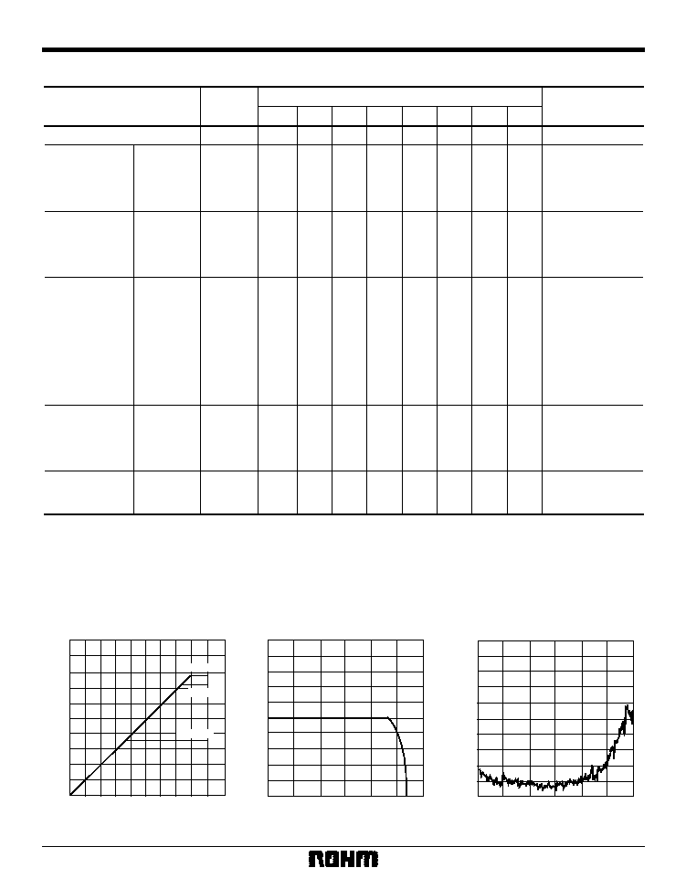
Electrical characteristic curves
OUTPUT VOLTAGE: V
OUT
(V
P-P
)
INPUT VOLTAGE: V
IN
(V
P-P
)
10
9
8
7
6
5
4
3
2
1
0
0
1
2
3
4
5
6
7
8
9
10
V
CC
= 12V
V
CC
= 9V
V
CC
= 5V
Fig. 2 V
IN
vs. V
OUT
(f = 1kHz)
VOLTAGE GAIN: C
f
(dB)
FREQUENCY: f (Hz)
≠ 4
100k
300k
1M
3M
10M
30M
100M
≠ 2
2
0
4
Fig. 3 Frequency characteristics
CROSSTALK: C
T
(dB)
FREQUENCY: f (Hz)
≠ 80
100k
300k
1M
3M
10M
30M
100M
≠ 60
≠ 40
≠ 20
0
20
Fig. 4 Interchannel crosstalk
5
Multimedia ICs
BA7649A / BA7649AF
∑
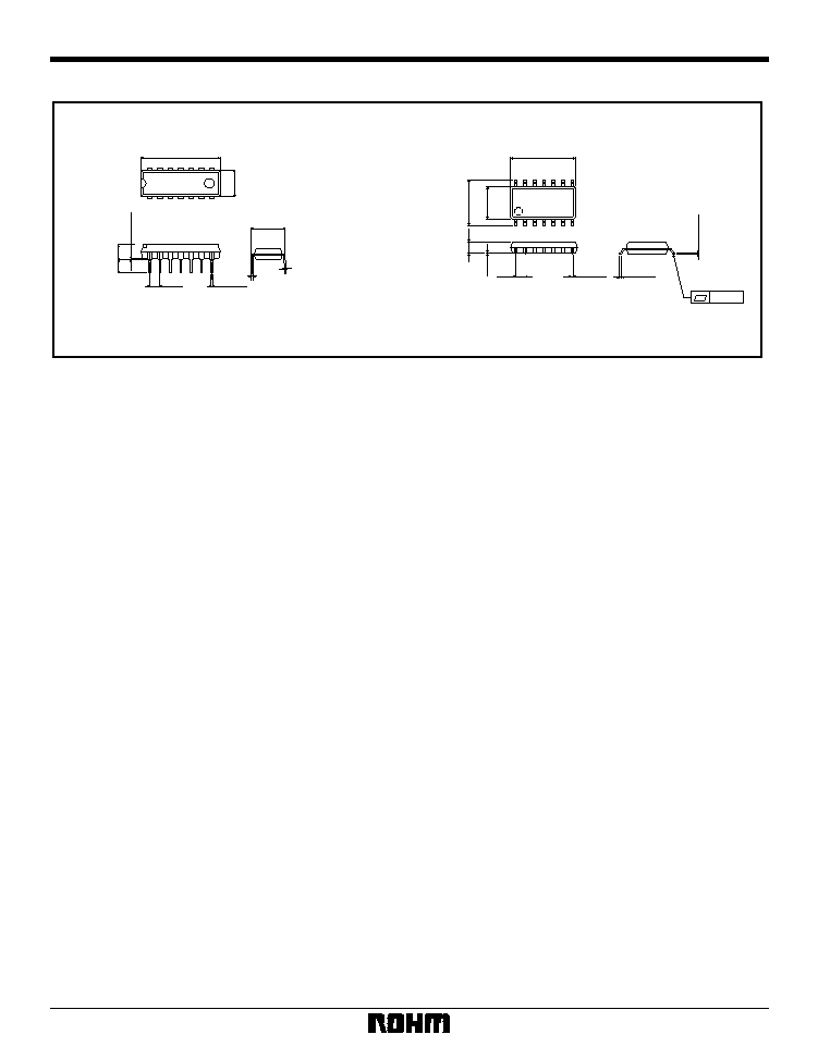
External dimensions (Units: mm)
BA7469A
BA7649AF
DIP14
SOP14
6.5
±
0.3
19.4
±
0.3
0.5
±
0.1
3.2
±
0.2
4.25
±
0.3
14
8
7
1
0.3
±
0.1
0.51Min.
7.62
0
∞
~ 15
∞
2.54
0.4
±
0.1
1.27
1
14
8.7
±
0.2
7
8
4.4
±
0.2
6.2
±
0.3
0.11
1.5
±
0.1
0.15
0.15
±
0.1
0.3Min.