1
Multimedia ICs
Video signal swither, 1
×
3-channel
with clamped-input
BA7652AF
The BA7652AF is a video-signal switching IC that contains a three-channel clamped-input multiplexer and a built-in
mute circuit. The inputs are sync-tip clamped (synchronous edge of the video input signals are aligned to the same
voltage), and as the input impedance is extremely large, it is possible to use a small value for the clamp capacitor.
[The recommended capacitor is 0.01
µ
F (FZ) ceramic].
·
Applications
Video cassette recorders and camcorders
·
Features
1) Small clamp capacitors can be used (ceramic,
3000pF (Min.), 0.01
µ
F (FZ) (recommended)).
2) Low supply voltage operation possible. Supply volt-
age range is 3.7V to 7.7V.
3) Superimposition used for fast switching speed with
low switching noise (70ns. Typ.).
4) Low power consumption
(when V
CC
= 5V, 25mW Typ.).
5) Wide dynamic range (3.1V
P-P
Typ. for V
CC
= 5V).
6) Mute function.
7) Excellent frequency characteristics
(10MHz, 0dB Typ.).
8) Low interchannel crosstalk ( 70dB Typ.).
9) Voltage can be applied to the control pins even
when V
CC
is not applied.
·
Absolute maximum ratings (Ta = 25°C)
Parameter
Symbol
Limits
Unit
V
CC
9
V
mW
°
C
°
C
500
Pd
Topr
Tstg
25 ~ + 75
55 ~ + 125
Applied voltage
Power dissipation
Operating temperature
Storage temperature
When mounted on a 50mm
×
50mm board, reduced by 5.0mW for each increase in Ta of 1
°
C over 25
°
C.
·
Recommended operating conditions (Ta = 25°C)
Parameter
Symbol
Limits
Unit
V
CC
4.0 ~ 7.0
V
Recommended operating voltage
2
Multimedia ICs
BA7652AF
·
Electrical characteristics (unless otherwise noted Ta = 25°C and V
CC
= 5.0V)
Parameter
Symbol
Unit
Conditions
Min.
Typ.
Max.
V
CC
3.7
--
--
--
7.7
V
I
CC
2.7
5.0
8.2
mA
V
om
2.6
3.1
--
V
P-P
G
V
0.5
0
dB
C
ta
70
dB
G
f
3.0
0
dB
V
TH L
--
--
1.0
V
V
TH H
2.5
--
--
V
TH
=
45
×
20 (V)
V
CC
V
F
f = 1MHz, V
IN
= 1.0V
P-P
f = 4.43MHz, V
IN
= 1.0V
P-P
f = 10MHz / 1MHz, V
IN
= 1.0V
P-P
f = 1kHz, THD = 1.0%
--
--
V
CC
CTL Threshold Level
0.5
1.0
Operating voltage
Supply current
Maximum output level
Voltage gain
Interchannel crosstalk
Frequency characteristic
CTL switching voltage
·
Guaranteed design parameters (unless otherwise noted Ta = 25°C and V
CC
= 5.0V)
Parameter
Symbol
Unit
Conditions
Min.
DG
--
0
0.5
%
DP
--
0.5
1.0
deg
Typ.
Max.
Differential gain
Differential phase
V
IN
= 1.0V
P-P
standard staircase signal
V
IN
= 1.0V
P-P
standard staircase signal
·
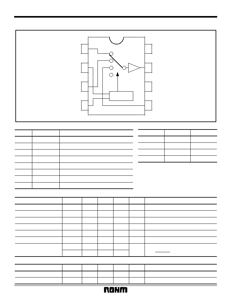
Pin descriptions
1
IN1
2
CTLa
3
IN2
4
CTLb
5
IN3
6
V
CC
7
OUT
8
GND
Pin No.
Name
Input 1
Control input a
Input 2
Control input b
Input 3
Supply voltage
Output
GND
Function
·
Control pin truth table
CTLa
CTLb
OUT
L
L
IN1
H
L
IN2
L
H
IN3
H
H
MUTE
·
Block diagram
1
2
3
4
8
7
6
5
IN1
CTLa
IN2
CTLb
GND
OUT
IN3
Logic
V
CC
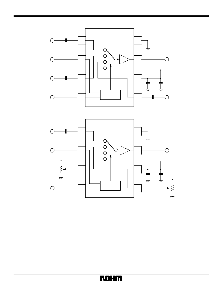
5
Multimedia ICs
BA7652AF
·
Application examples
1
2
3
4
8
7
6
5
IN1
CTLa
IN2
CTLb
GND
OUT
IN3
LOGIC
Logic
Logic
C.Video IN
C.Video IN
C.Video OUT
C.Video IN
V
CC
0.01
µ
F
0.01
µ
F
47
µ
F
0.1
µ
F
0.01
µ
F
V
CC
+
When superimposition is used
1
2
3
4
8
7
6
5
IN1
CTLa
IN2
CTLb
GND
OUT
IN3
LOGIC
Logic
Logic
DC1.7V or more
DC1.7V or more
C.Video IN
C.Video or DC OUT
0.01
µ
F
47
µ
F
0.1
µ
F
V
CC
V
CC
Fig. 1
+
·
Operation notes
(1) To ensure stable clamp operation, the output
impedance of the previous stage connected to the
inputs should be 1k
or lower.
(2) If large input clamp capacitors are used, the time
constant of the circuit will mean that some time will be
required until stable operation after power is applied.
The value for the input clamp capacitors is 0.1
µ
F max.
(0.01
µ
F (FZ) ceramic capacitor recommended) .
(3) The BA7652AF is a three-channel multiplexer, but
two-channel operation is also possible. In this case, if
the unused input is left open it will oscillate, but this will
not effect the other inputs and cause problems. If this is
a concern, ground the unused input via a capacitor, or
connect it directly to V
CC
.
(4) If control inputs are left open they will be unstage,
set to H or L.
(5) When using superimposition, the DV voltage direct-
ly applied to the inputs should be at least 1.7V.