1
Multimedia ICs
2-input, 1-output video signal
switcher
BA7654F
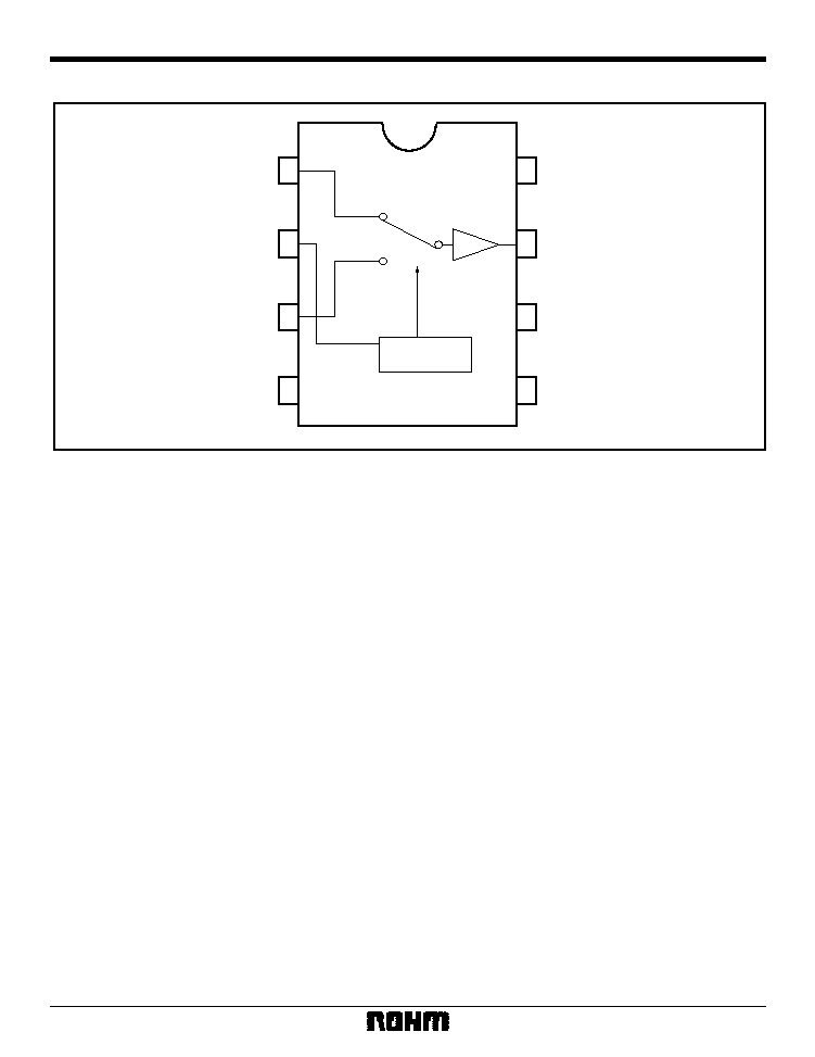
The BA7654F is video signal switch consisting of two input pins (IN1 and IN2), one CTL pin (CTL), and one output
pin (OUT). The inputs are sync-tip clamped (synchronous edge of the video input signals are aligned to the same
voltage), and as the input impedance is extremely large, it is possible to use a small value for the clamp capacitor
(the recommended capacitor is 0.01
µ
F (FZ) ceramic).
∑
Applications
VCRs, TVs, and other equipment using video signals
∑
Features
1) Small clamp capacitors can be used (ceramic,
3000pF (Min.), 0.01
µ
F (FZ) (recommended)).
2) Low supply voltage operation possible supply volt-
age range is 3.7V to 7.7V.
3) Superimposition used for fast switching speed with
low switching noise (70ns Typ.).
4) Low power consumption
(when V
CC
= 5V, 25mW Typ.).
5) Wide dynamic range (when V
CC
= 5V, 3.1V
P-P
Typ.).
6) Excellent frequency characteristics (10MHz, 0dB
Typ.).
7) Low interchannel crosstalk (≠ 70dB Typ.).
8) Voltage can be applied to the control pins even
when V
CC
is not applied.
∑
Selected output mode setting table
CTL
OUT
L
IN1
H
IN2
∑
Absolute maximum ratings (Ta = 25∞C)
Parameter
Symbol
Limits
9
500
≠ 25 ~ + 75
≠ 55 ~ + 125
Unit
V
mW
∞
C
∞
C
V
CC
Pd
Topr
Tstg
Applied voltage
Power dissipation
Operating temperature
Storage temperature
Reduced by 50mW for each increase in Ta of 1
∞
C over 25
∞
C.
∑
Recommended operating conditions (Ta = 25∞C)
Parameter
Symbol
Limits
4.0 ~ 7.0
Unit
V
V
CC
Operating power supply voltage
Not designed for radiation resistance.
5
Multimedia ICs
BA7654F
∑
Electrical characteristics (unless otherwise noted, Ta = 25∞C, V
CC
= 5V)
Parameter
Symbol
Min.
3.7
2.7
2.6
≠ 0.5
Typ.
--
5.0
3.1
0
Max.
7.7
8.2
--
+ 0.5
V
CC
I
CC
Vom
G
V
Power supply voltage
Circuit current
Maximum output level
Voltage gain
Interchannel crosstalk
Frequency characteristics
CTL switching voltage
Unit
V
mA
V
P-P
dB
Conditions
f = 1kHz, THD = 1.0%
f = 1MHz, V
IN
= 1.0V
P-P
≠ 3.0
0
+ 1.0
Gf
dB
V
f = 10MHz/1MHz, V
IN
= 1.0V
P-P
--
--
1.0
VthL
2.5
--
--
VthH
--
≠ 70
--
Cta
dB
f = 4.43MHz, V
IN
= 1.0V
P-P
Vcc-CTL Threshold Level
Vth =
◊
20 (V)
Vcc-V
F
45
--
--
∑
Guaranteed design parameters (unless otherwise noted, Ta = 25∞C, V
CC
= 5V)
Parameter
Symbol
Min.
--
Typ.
0
Max.
0.5
DG
Differential gain
Differential phase
Unit
%
--
0.5
1.0
DP
deg
Conditions
V
IN
= 1.0V
P-P
standard staircase signal
V
IN
= 1.0V
P-P
standard staircase signal
∑
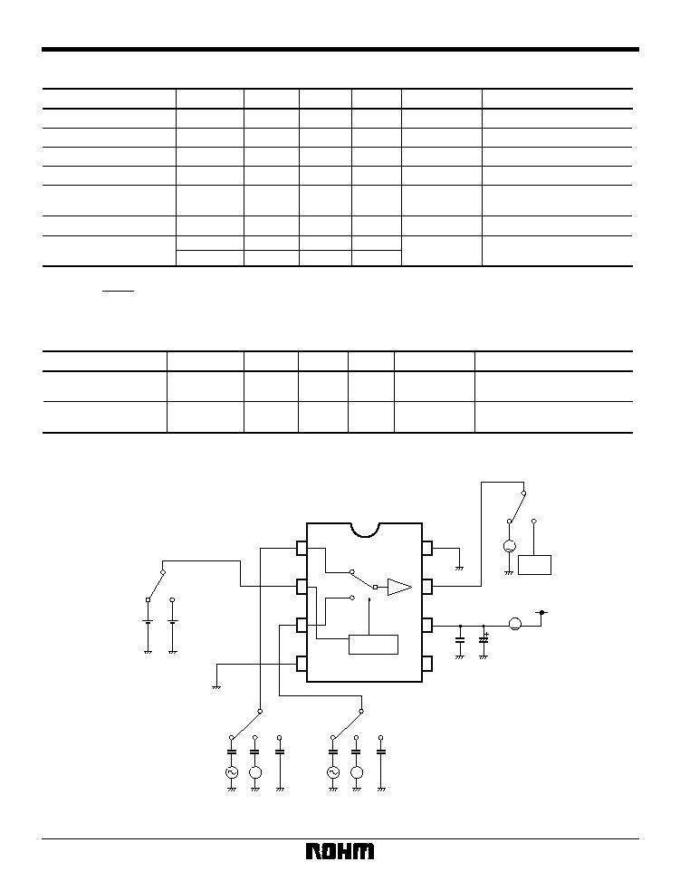
Measurement circuit
1
8
2
7
3
6
4
5
L o g i c
Clump
Clump
SW7
1
2
Vector
Scorp
Vcc
SW2
1
2
47
µ
0.1
µ
C11
C10
Open
2.5V
1.0V
SW1
1
2
OSC
C1
C2
3
C3
3300p
3300p
3300p
1.0V
V
A
SG
SW3
1
2
OSC
C4
C5
3
C6
3300p
3300p
3300p
SG
Fig. 1