 | –≠–ª–µ–∫—Ç—Ä–æ–Ω–Ω—ã–π –∫–æ–º–ø–æ–Ω–µ–Ω—Ç: BA7657S | –°–∫–∞—á–∞—Ç—å:  PDF PDF  ZIP ZIP |
1
Multimedia ICs
Input selector switch for high
definition displays
BA7657F / BA7657S
The BA7657F and BA7657S are for high definition displays, and have internal switches for switching between broad-
band RGB signals and HD / VD signals, as well as an internal synchronization separator. These ICs simplify the de-
signing of input units for deluxe displays.
∑
Applications
CRT display, HDTV, video board for personal computer, etc.
∑
Features
1) Operates on a single 5V power supply.
2) Internal broadband RGB switch (frequency charac-
teristics: 230MHz, ≠ 3dB).
3) Internal HD / VD switch.
4) Internal synchronization separator for synchronizing
signals superimposed onto G signals.
∑
Absolute maximum ratings (Ta = 25∞C)
∑
Recommended operating conditions (Ta = 25∞C)
Parameter
Symbol
Limits
Unit
Power supply voltage
V
CC
8.0
V
Power
dissipation
BA7657F
550
mW
BA7657S
1200
Operating temperature
Topr
∞
C
Storage temperature
Tstg
∞
C
Pd
≠ 25 ~ + 75
≠ 55 ~ + 125
Reduced by 5.5mW (BA7657F) or 12mW (BA7657S) for each increase in Ta of 1
∞
C over 25
∞
C.
Parameter
Symbol
Min.
Typ.
Max.
Unit
Power supply voltage
V
V
CC
4.5
5.0
5.5
2
Multimedia ICs
BA7657F / BA7657S
∑
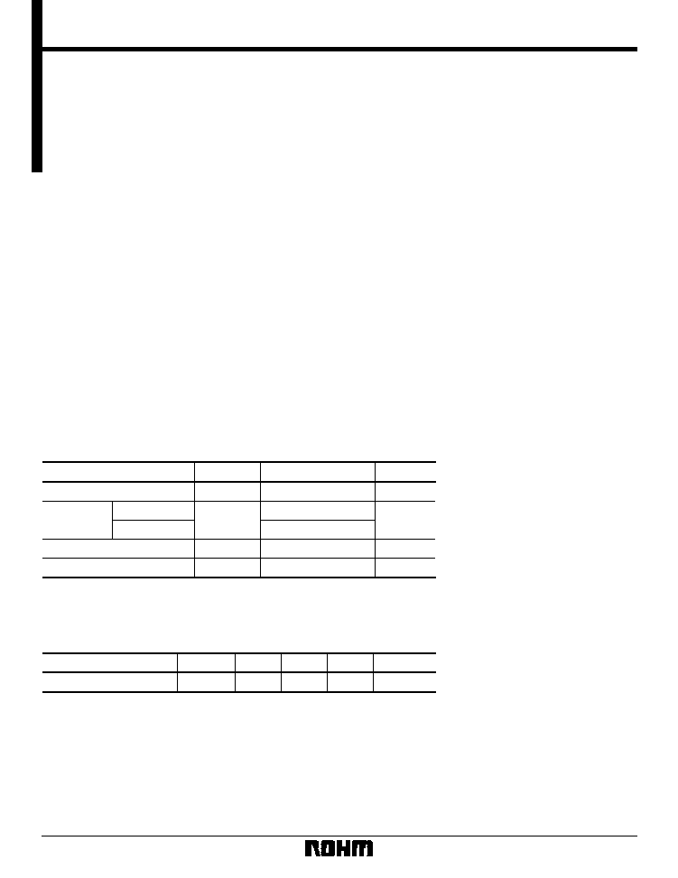
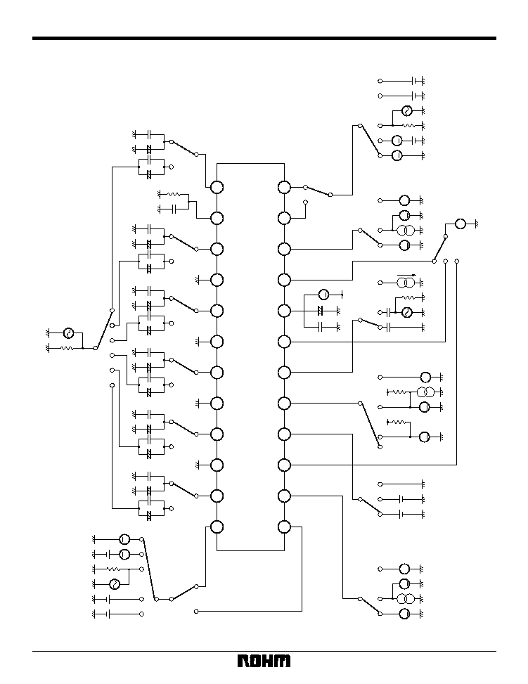
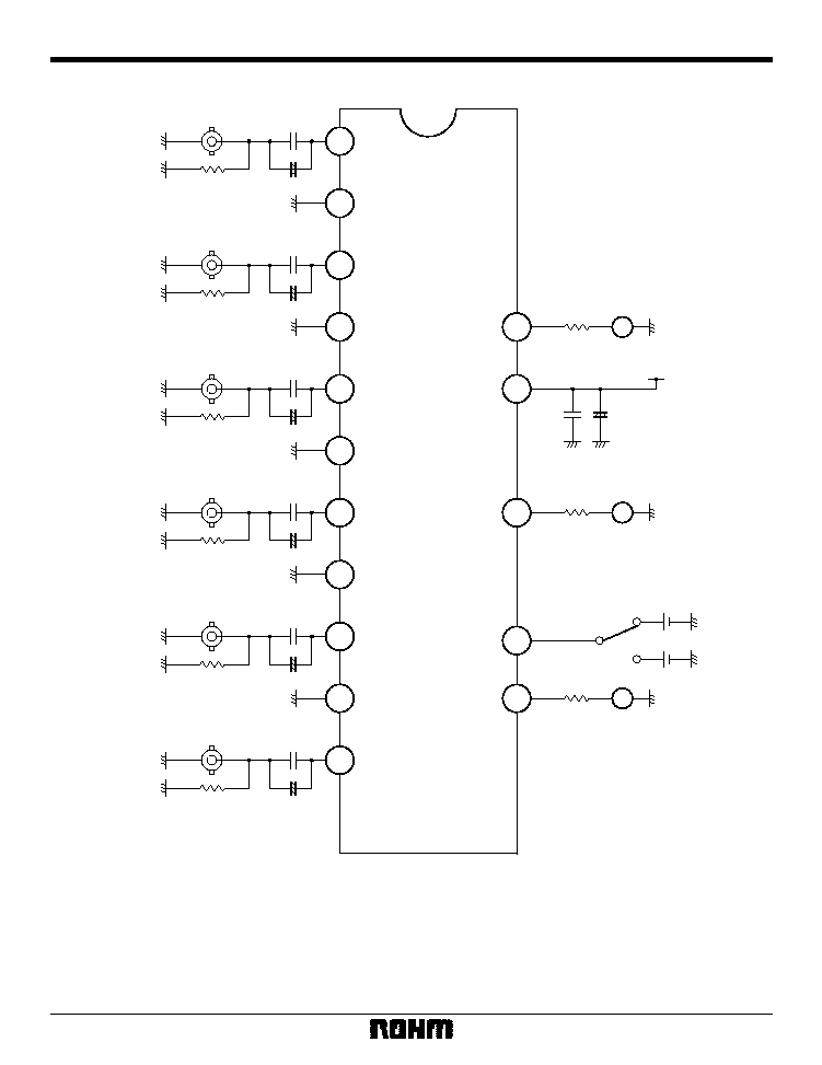
Block diagram
1
2
3
4
5
6
7
8
9
10
11
12
24
23
22
21
20
19
18
17
16
15
14
13
1
2
1
2
1
2
1
2
1
2
DET
Logic
Syncsepa
Ground
Ground
Ground
Ground
V
CC
CTL (H: IN1, L: IN2)
Red 1 input
Green 1 input
Blue 1 input
Red 2 input
Green 2 input
Blue 2 input
VD 1 input
VD 2 input
VD output
Blue output
Composite sync output
Composite video input (Sync on Green)
Green output
Red output
HD output
HD 2 input
HD 1 input
HD Sync signal detector
3
Multimedia ICs
BA7657F / BA7657S
∑
Pin descriptions
Pin name
1
Red 1 input
Color signal R1 input
2
detector
HD Sync signal Detecting phase of the synchronization
signal detector circuit
3
Green 1 input
Color signal G1 input
4
Ground
Ground
5
Blue 1 input
Color signal B1 input
6
Ground
Ground
7
Red 2 input
Color signal R2 input
8
Ground
Ground
9
Green 2 input
Color signal G2 input
10
Ground
Ground
11
Blue 2 input
Color signal B2 input
VD 1 input
Vertical synchronization signal VD1 input
14
VD output
Vertical synchronization signal VD output
15
Blue output
Color signal B output
16
Control
Control (high = IN1, low = IN2)
17
output
Composite sync
Synchronization signal output
18
input
Composite video Composite signal input
(Sync on Green)
19
Green output
Color signal G output
20
V
CC
Power supply
21
Red output
Color signal R output
22
HD output
Horizontal synch. signal HD output
23
HD 2 input
Horizontal synch. signal HD2 input
24
HD 1 input
Horizontal synch. signal HD1 input
Pin name
13
VD 2 input
Vertical synchronization signal VD2 input
Function
Pin No.
Function
Pin No.
12
∑
Output selection setting table
CTL
R
G
B
HD
VD
H
IN1
IN1
IN1
IN1
IN1
L
IN2
IN2
IN2
IN2
IN2
∑
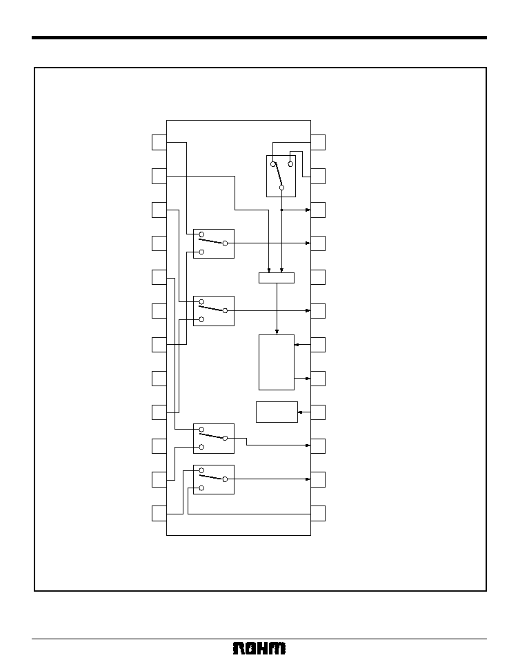
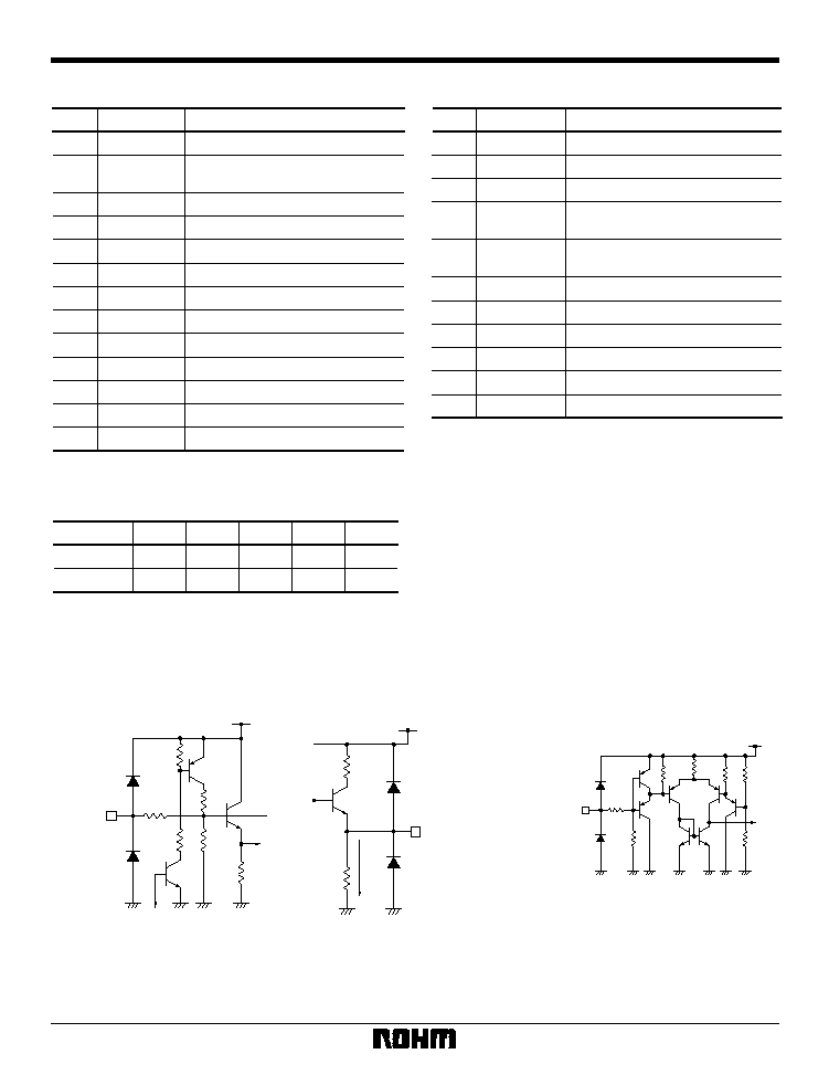
Input / output circuits
1, 3, 5
7, 9, 11pin
6.8k
21k
1k
100
V
CC
R. G. B input
15, 19, 21pin
400
50
5mA
V
CC
R. G. B output
12, 13
23, 24pin
15k
35k
1k
50k
V
CC
HD. VD input
4
Multimedia ICs
BA7657F / BA7657S
14, 22pin
100
1.2k
2.0k
V
CC
15k
660
HD. VD output
16pin
1k
50k
35k
15k
V
CC
Control
2pin
25k
25k
V
CC
from HD out
to sync sepa
HD sync signal detector
18pin
25k
25k
50
µ
A
V
CC
100
from DET out
Composite Video input
17pin
V
CC
Composite Sync output
5
Multimedia ICs
BA7657F / BA7657S
∑
Electrical characteristics (unless otherwise noted, Ta = 25∞C, V
CC
= 5.0V)
Parameter
Symbol
Min.
Typ.
Max.
Unit
Conditions
Measurement circuit
Maximum output level
V
om
--
--
V
P-P
f = 1kHz
Fig.1
Voltage gain
G
V
≠ 1.0
≠ 0.5
0
dB
f = 1MHz, V
IN
= 1V
P-P
Fig.1
Input pin voltage gain deviation
G
VI
≠ 0.2
0
0.2
dB
f = 1MHz, V
IN
= 1V
P-P
Fig.1
Block voltage gain deviation
G
VB
≠ 0.2
0
0.2
dB
f = 1MHz, V
IN
= 1V
P-P
Fig.1
Input pin crosstalk 1
CTI1
--
≠ 50
≠ 40
dB
f = 10MHz, V
IN
= 1V
P-P
Fig.2
Block crosstalk 1
CTB1
--
≠ 50
≠ 40
dB
f = 10MHz, V
IN
= 1V
P-P
Fig.2
Digital switch unit
Input high level voltage
Analog switch unit
1.8
--
--
V
Fig.1
Input low level voltage
--
--
1.2
V
Fig.1
Input high level current
80
100
130
µ
A
V
IN
= 5.0V
Fig.1
Input low level current
--
µ
A
V
IN
= 0V
Fig.1
Rise time
T
R
--
30
50
ns
Fig.1
Fall time
--
30
50
ns
Fig.1
Rise delay time
--
50
80
ns
Fig.1
Fall delay time
--
30
50
ns
Fig.1
Output high level voltage
3.0
3.7
--
V
Fig.1
Output low level voltage
--
0.2
0.4
V
Fig.1
Output high level current
≠ 3
≠ 1
≠ 400
--
--
µ
A
Fig.1
Output low level current
5
--
--
mA
Fig.1
SYNC separation unit
Minimum SYNC
separation level
V
SMin.
--
mV
P-P
Fig.1
Output high level voltage
4.5
5.0
--
V
Fig.1
Output low level voltage
--
0.2
0.5
V
Fig.1
Output low level current
2
--
--
mA
Fig.1
Rise time
T
R
--
80
130
ns
Fig.1
Fall time
T
F
--
30
80
ns
Fig.1
Rising delay time
T
RD
--
100
150
ns
Fig.1
Fall delay time
T
FD
--
100
150
ns
Fig.1
Control unit
Output high level voltage
1.8
--
--
V
Fig.1
Output low level voltage
--
--
1.2
V
Fig.1
Output high level current
80
100
130
µ
A
V
IN
= 5.0V
Fig.1
Output low level current
--
µ
A
V
IN
= 0V
Fig.1
V
IH
V
IL
I
IH
I
IL
T
F
T
RD
T
FD
V
OH
V
OL
I
OH
I
OL
V
OH
V
OL
I
OL
V
IH
V
IL
I
IH
I
IL
Quiescent current
I
CC
20
35
50
mA
Fig.1
2.8
50
≠ 3
≠ 1
≠ 50
6
Multimedia ICs
BA7657F / BA7657S
∑
Guaranteed design parameters (unless otherwise noted, Ta = 25∞C, V
CC
= 5.0V)
Parameter
Symbol
Min.
Typ.
Max.
Unit
Conditions
Measurement circuit
Input pin crosstalk 2
Analog switch unit
CTI2
--
dB
Fig.2
Block crosstalk 2
CTB2
--
dB
Fig.2
Frequency characteristic deviation
Gf
dB
Fig.2
Input pin frequency characteristic deviation
GfI
0
dB
Fig.2
Block frequency characteristic deviation
GfB
0
≠ 30
≠ 15
≠ 30
≠ 15
≠ 6
≠ 3
≠ 1
≠ 1
+ 1
≠ 1
+ 1
dB
Fig.2
f = 230MHz, V
IN
= 1V
P-P
f = 230MHz, V
IN
= 1V
P-P
f = 1MHz / 230MHz, V
IN
= 1V
P-P
f = 1MHz / 100MHz, V
IN
= 1V
P-P
f = 1MHz / 100MHz, V
IN
= 1V
P-P
SYNC separation frequency
fH-R
200
--
--
kHz
input waveform
1
Fig.3
SYNC separation pulse width 1
pwH1
3.0
--
--
µ
s
input waveform
2
fH = 20kHz
Fig.3
SYNC separation pulse width 2
pwH2
0.5
--
--
µ
s
input waveform
2
fH = 100kHz
Fig.3
SYNC separation pulse width 3
pwH3
0.3
--
--
µ
s
input waveform
2
fH = 200kHz
Fig.3
SYNC separation level 1
SYNC separation unit
VS1
300
--
--
µ
s
input waveform
3
fH = 20kHz
Fig.3
SYNC separation level 2
VS2
100
--
--
µ
s
input waveform
3
fH = 100kHz
Fig.3
SYNC separation level 3
VS3
60
--
--
µ
s
input waveform
3
fH = 200kHz
Fig.3
Input waveform (input to pin 3 or 9 [see illustration to right], Ro = 240
)
1 Vs and pwH = variable. Vs and pwH are interrelated. Refer to characteristics graph.
2 Vs = 130mV, pwH = variable
3 pwH = 1
µ
s, Vs = variable
Duration of horizontal synchronization signal
Duty 25%
Vr = 0.7V
Vs = 130mV
pwH = 1
µ
s
(1H)
7
Multimedia ICs
BA7657F / BA7657S
∑
Measurement circuit
1
2
3
4
5
6
7
8
9
10
11
12
24
23
22
21
20
19
18
17
16
15
14
13
C1
C2
C1
C2
1
2
SW2
C1
C1
C1
C1
C2
C2
C2
C2
C1
C1
C1
C1
C2
C2
C2
C2
1
1
1
1
2
2
2
2
1
2
3
4
5
SW9 SW8
1
2
A
75
OSC2
1.2V
1.8V
5V
C1
C2
C1
C2
1
2
SW1
470pF
SW3
SW4
SW5
SW6
75
1
2
3
4
5
OSC1
SW7
47
µ
F
0.01
µ
F
1
2
3
SW14
Oscilloscope
Network
Analyzer
1
2
1
2
3
Oscilloscope
1
3
4
5
2
75
1.2V
1.8V
5V
SW17
SW16
2
75
OSC3
1
µ
F
1
µ
F
1
3
20
µ
A
3
Oscilloscope
2k
V
CC
= 5V
4
2k
V
CC
= 5V
2
1
1.2V
1
2
3
1.8V
SW12
SW11
1
2
3
Oscilloscope
SW10
SW15
470k
6
C1: 0.01
µ
F
C2: 47
µ
F
OSC5
A
V
CC
= 5V
V
V
V
V
V
V
A
A
A
Fig. 1
+
+
+
+
+
+
+
+
+
+
+
+
+
8
Multimedia ICs
BA7657F / BA7657S
∑
Electrical characteristic measurement conditions (1 / 2)
Parameter
Switch condition
11
Other
Supply current
3
1
Analog switch unit
(listings for color signal R switches only)
Parameter
Switch condition
1
2
3
4
5
6
7
11
14
Other
Maximum output level R1
2
1
1
1
1
1
1
1
1
1
Maximum output level R2
1
2
1
1
1
1
1
2
1
1
Voltage gain R1
2
1
1
1
1
1
1
1
1
1
Voltage gain R2
1
2
1
1
1
1
1
2
1
1
Digital switch unit
(listings for synchronization signal VD switches only)
Parameter
Switch condition
8
9
10
11
15
16
17
Other
Input voltage VD1, "H" level
1
4
1
1
1
1
1
1
Input voltage VD2, "H" level
2
4
1
2
1
1
1
1
Input voltage VD1, "L" level
1
5
1
1
1
1
1
1
Input voltage VD2, "L" level
2
5
1
2
1
1
1
1
Input current VD1, "H" level
1
2
1
1
1
1
1
1
Input current VD2, "H" level
2
2
1
2
1
1
1
1
Input current VD1, "L" level
1
1
1
1
1
1
1
1
Input current VD2, "L" level
2
1
1
2
1
1
1
1
Rise time
1
3
3
1
1
1
1
1
Fall time
1
3
3
1
1
1
1
1
Rise delay time
1
3
3
1
1
1
1
1
Fall delay time
1
3
3
1
1
1
1
1
Output voltage, "H" level
1
2
1
1
1
1
1
1
Output voltage, "L" level
1
1
1
1
1
1
1
1
Output current, "H" level
1
2
2
1
1
1
1
1
Output current, "L" level
1
1
2
1
1
1
1
1
9
Multimedia ICs
BA7657F / BA7657S
SYNC separation unit
Parameter
Switch condition
12
13
Other
Minimum SYNC
separation level
4
2
1
Output voltage, "H" level
2
3
1
Output voltage, "L" level
2
1
1
1
Output current, "L" level
3
1
1
1
Rise time
4
2
1
Fall time
4
2
1
Rise delay time
4
2
1
Fall delay time
4
2
1
10
Multimedia ICs
BA7657F / BA7657S
∑
Measurement circuit for frequency characteristics and crosstalk characteristics
1
C2
C1
2
C2
C2
C2
C2
C2
C1
C1
C1
C1
C1
3
4
5
6
7
8
9
10
11
0.01
µ
F
47
µ
F
21
20
240
240
Network
Analyzer
Network
Analyzer
19
240
Network
Analyzer
15
SW
2
1
1.8V
1.2V
C1: 0.01
µ
F
C2: 47
µ
F
16
50
50
50
50
50
50
V
CC
= 5V
Fig. 2
+
+
+
+
+
+
+
11
Multimedia ICs
BA7657F / BA7657S
∑
Procedure for measurement of frequency characteristics and crosstalk characteristics
∑
Circuit operation
Relationship between inputs and outputs
(1) Frequency characteristics
Use an oscillator to input a sine wave (V
IN
= 1.0V
P-P
, f =
1MHz / 230MHz) to the color signal pins.
To select R1, G1 and B1: Set the switch to 1.
To select R2, G2 and B2: Set the switch to 2.
Gf1 = Gv (f = 1MHz) ≠ Gv (230MHz) [dB]
(2) Frequency characteristic deviation
Use an oscillator to input a sine wave (V
IN
= 1.0V
P-P
, f =
1MHz / 100MHz) to the color signal pins.
To select R1, G1 and B1: Set the switch to 1.
To select R2, G2 and B2: Set the switch to 2.
Gf1 = Gv (f = 1MHz) ≠ Gv (100MHz) [dB]
Gfl = Gf (IN1) ≠ Gf (IN2) [dB]
GfB = Gf (R1) ≠ Gf (G1), Gf (G1) ≠ Gf (B1),
Gf (B1) ≠ Gf (R1) [dB]
(3) Input pin crosstalk (1)
Use an oscillator to input a sine wave (V
IN
= 1.0V
P-P
, f =
10MHz) to IN1.
Use a capacitor to connect IN2 to GND. Set the switch
to 2, then select output IN2 and measure.
CTI1 = 20log (V
OUT
/ V
IN
) [dB]
(4) Input pin crosstalk 2
Use an oscillator to input a sine wave (V
IN
= 1.0V
P-P
, f =
230MHz) to IN1.
Connect IN2 to the ground through a capacitor.
Set the switch to 2, input to IN2, then measure.
CTI2 = 20log (V
OUT
/ V
IN
) [dB]
(5) Block crosstalk 1
Use an oscillator to input a sine wave (V
IN
= 1.0V
P-P
, f =
10MHz) to G1 and B1.
Connect R1 to the ground through a capacitor.
Set the switch to 1 and measure the R output.
CTB1R = 20log (V
OUT
R / V
IN
G1) [dB]
Similarly,
CTB1G = 20log (V
OUT
G / V
IN
B1) [dB]
CTB1B = 20log (V
OUT
B / V
IN
R1) [dB]
(6) Block crosstalk 2
Use an oscillator to input a sine wave (V
IN
= 1.0V
P-P
, f =
230MHz) to G1 and B1.
Connect R1 to the ground through a capacitor.
Set the switch to 1 and measure the R output.
CTB2R = 20log (V
OUT
R / V
IN
G1) [dB]
Similarly,
CTB2G = 20log (V
OUT
G / V
IN
B1) [dB]
CTB2B = 20log (V
OUT
B / V
IN
R1) [dB]
(1) Analog switches
Used for switching between the two sets of RGB color
signals. Connect the high voltage to CTL to select IN1,
or the low voltage to select IN2.
(2) Digital switches
Used for switching between the two sets of HD / VD
synchronization signals. Connect the high voltage to
CTL to select the HD / VD synchronization signal for
IN1, or the low voltage to select the HD / VD synchro-
nization signal for IN2.
(3) Synchronization separator
Used to output the synchronization signal after separat-
ing it from the composite signal (Sync on Green).
When the HD signal is input it activates the synchro-
nization signal detector, stopping the synchronization
separator. The length of time that the synchronization
separator remains stopped is set according to the con-
stant attached to the detector wave pin of the synchro-
nization detector.
Output
HD
VD
Sync on Green
HD
VD Composite Sync
--
--
--
--
--
--
--
--
--
--
--
--
--
--
--
--
--
--
--
--
Input
12
Multimedia ICs
BA7657F / BA7657S
∑
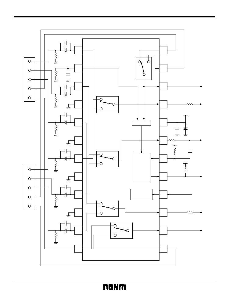
Application example
1
2
3
4
5
6
7
8
9
10
11
12
24
23
22
21
20
19
18
17
16
15
14
13
1
2
1
2
1
2
1
2
1
2
DET
Logic
Syncsepa
R
G
B
H
V
R
G
B
H
V
IN1
IN2
Ro
Ro
Composite Sync OUT
CTL
IN1: H
IN2: L
Ro
Blue OUT
V
CC
5V
Green OUT
Red OUT
HD OUT
VD OUT
0.01
µ
75
470p
75
470K
75
75
75
75
0.01
µ
68k
2k
47
µ
/ 6.3V
1
µ
0.01
µ
47
µ
/ 6.3V
47
µ
/ 6.3V
47
µ
/ 6.3V
47
µ
/ 6.3V
47
µ
/ 6.3V
47
µ
/ 6.3V
0.01
µ
0.01
µ
0.01
µ
0.01
µ
V
CC
5V
V
CC
5V
Fig. 3
+
+
+
+
+
+
+

13
Multimedia ICs
BA7657F / BA7657S
∑
External dimensions (Units: mm)
SOP24
SDIP24
0.15
0.11
1.8 ± 0.1
5.4 ±
0.2
7.8 ± 0.3
0.4 ± 0.1
15.0 ± 0.2
0.3Min.
0.15 ±
0.1
24
1
13
12
1.27
0.51Min.
6.5 ±
0.3
0.3 ± 0.1
7.62
3.4 ± 0.2
22.9 ± 0.3
0.5 ± 0.1
1.778
13
12
24
1
3.95 ± 0.3
0∞ ~ 15∞
BA7657F
BA7657S
Resistors attached to analog switch outputs
Because analog switch frequency characteristics de-
pend on output load capacity, set external resistance
(Ro) so that the frequency characteristics remain flat. A
too-large resistance will suppress the characteristic
peak.
∑
Operation notes
∑
Electrical characteristic curves
1M
10M
100M
300M
0
2
4
FREQUENCY: f (Hz)
≠ 2
≠ 4
≠ 6
≠ 8
≠ 10
≠ 12
≠ 14
VOLTAGE GAIN: G
V
(dB)
Fig. 4 Frequency characteristics
sink level Vs
280mV
50mV
Duty25%
10.0
9.0
8.0
7.0
6.0
5.0
4.0
3.0
2.0
1.0
0.0
20
40
60
80 100 120 140 160 180 200
FREQUENCY: fH (kHz)
130mV
PULSE WIDTH: pwH (
µ
s)
Fig. 6 Minimum SYNC
separation characteristics
1M
10M
100M
300M
10
0
CROSSTALK: CT (dB)
FREQUENCY: f (Hz)
≠ 10
≠ 20
≠ 30
≠ 40
≠ 50
≠ 60
≠ 70
≠ 80
≠ 90
Fig. 5 Interchannel crosstalk characteristics