 | –≠–ª–µ–∫—Ç—Ä–æ–Ω–Ω—ã–π –∫–æ–º–ø–æ–Ω–µ–Ω—Ç: BA7660FS | –°–∫–∞—á–∞—Ç—å:  PDF PDF  ZIP ZIP |
1
Multimedia ICs
3-channel 75
driver
BA7660FS
The BA7660FS is a 75
driver with a 6dB amplifier and three internal circuits, and provides 75
drive of composite
Y signals and C signals, as well as RGB signals. Each load is capable of driving two circuits, and a sag correction
function reduces the capacitance of the output coupling capacitor.
The input voltage is within a range of 0V to 1.5V, enabling direct connection of ordinary D / A converter output. An
internal power-saving circuit is also included which provides simultaneous muting on all three channels, and output
pin shorting protection.
∑
Applications
DVDs, set top boxes and other digital video devices
∑
Features
1) Can be coupled directly to D / A converter output.
2) Operates at a low power consumption (115mW typ.).
3) Internal output muting circuit.
4) Internal power-saving circuit.
5) Internal output protection circuit.
6) An internal sag correction function makes it possible
to reduce the capacitance of the output coupling
capacitor.
7) Each load is capable of driving two circuits.
8) The compact 16-pin SSOP-A package is used.
∑
Absolute maximum ratings (Ta = 25∞C)
Parameter
Symbol
Vcc
Pd
Topr
Tstg
Limits
Unit
8
650
≠ 25 ~ + 75
≠ 55 ~ + 125
V
mW
∞
C
∞
C
Power supply voltage
Power dissipation
Operating temperature
Storage temperature
∑
Recommended operating conditions (Ta = 25∞C)
Parameter
Symbol
Vcc
Min.
4.5
Typ.
5.0
Max.
5.5
Unit
V
Operating power supply voltage
2
Multimedia ICs
BA7660FS
∑
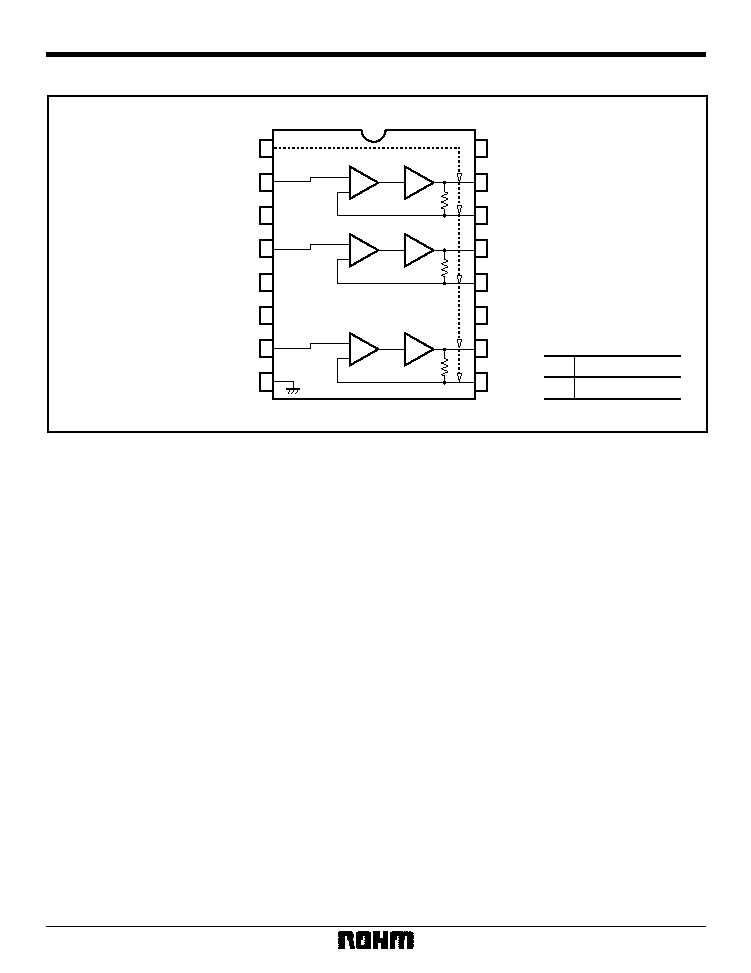
Block diagram
MUTE
INA
GND
INB
GND
N.C.
INC
GND
1
2
3
4
5
6
7
8
16
15
14
13
12
11
10
9
OUTA1
V
CC
OUTA2
OUTB1
OUTB2
N.C.
OUTC1
OUTC2
75
6dB
75
6dB
6dB
75
H
3ch MUTE
MUTE (1pin)
NORMAL
L
3
Multimedia ICs
BA7660FS
∑
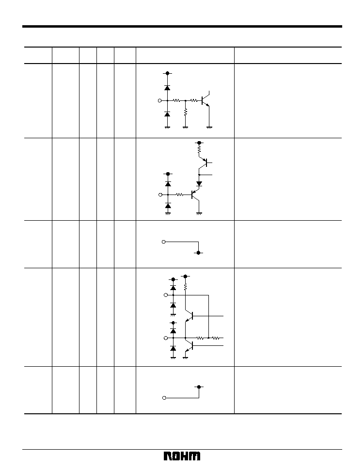
Pin descriptions and input / output circuits
Pin. No
Pin name
IN
OUT
Reference
voltage
Equivalent circuit
Function
1
MUTE
K
--
--
K
--
--
2
4
7
INA
INB
INC
--
K
0.9V
0.95V
14
12
9
15
13
10
OUTA2
OUTB2
OUTC2
OUTA1
OUTB1
OUTC1
--
--
5.0V
16
V
CC
Muting control
If MUTE (pin 1) is set to HIGH, muting
is carried out simultaneously on all
three channels.
Signal input
Input signals consist of composite
video signals, Y signals, C signals,
RGB, and others. The input level is
within a range of 0 to 1.3 (min.) to 1.5
(typ.).
--
--
0V
3
5
8
GND
Ground
Signal output
The signal output level is (0.9 + 2
◊
input voltage [V]). Pins 9, 12, and 14
are the pins for sag correction. If pins
10, 13, and 15 are set to 0.2V or less,
the protective circuit is triggered and
the power-saving mode is accessed.
Power supply
15k
8k
GND
15pin
13pin
10pin
14pin
12pin
9pin
Vcc
4
Multimedia ICs
BA7660FS
∑
Electrical characteristics (unless otherwise noted, Ta = 25∞C, V
CC
= 5V)
Parameter
Symbol
Min.
Typ.
Max.
Unit
Conditions
Circuit current
I
CC
11.4
22.8
34.2
mA
Maximum output level
Vom
2.6
3.0
--
V
P- P
Voltage gain
G
V
5.5
6.0
6.5
dB
Frequency characteristic
G
f
1.0
0.0
1.0
dB
Muting attenuation
With no signal
f = 1kHz,THD = 1%
f = 4.43MHz,1V
P- P
f = 7MHz / 1MHz,1V
P- P
f = 4.43MHz,1V
P- P
M
T
--
60
--
dB
Muting switching level HIGH
V
THH
3.5
--
V
CC
V
Muting switching level LOW
V
THL
0
--
1.0
V
≠
≠
--
--
∑
Measurement circuit
1
2
3
4
5
6
7
8
75
6dB
75
6dB
75
6dB
16
15
14
13
12
11
10
9
SW1
SW2
2
3.3V
1
1.2V
3
1
µ
F
1
430k
75k
SW4
N.C.
SW7
SW16
2
V
CC
1
0.1
µ
F
47
µ
F
N.C.
100
µ
F
22
µ
F
75
75
75
1
µ
F
2
1
µ
F
1
430k
75k
1
µ
F
2
1
µ
F
1
430k
75k
1
µ
F
2
V
A
100
µ
F
22
µ
F
V
100
µ
F
22
µ
F
V
∑
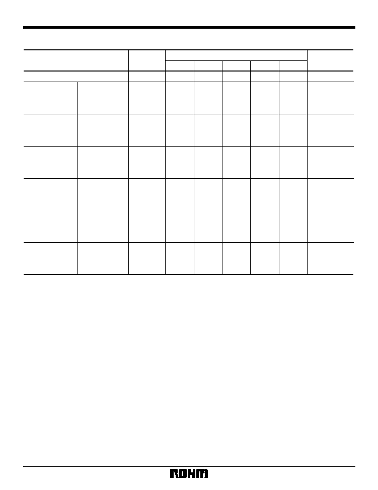
Guaranteed design parameters (unless otherwise noted, Ta = 25∞C, V
CC
= 5V)
Parameter
Symbol
Min.
Typ.
Max.
Unit
Conditions
Differential gain
DG
--
0.5
1.5
%
Differential phase
DP
--
0.5
1.5
deg
Interchannel crosstalk
C
T
--
60
55
dB
Interchannel voltage gain
differential
G
V
0.5
0.0
0.5
dB
1.0V
P- P
reference staircase signal
1.0V
P- P
reference staircase signal
f = 4.43MHz,1V
P- P
f = 4.43MHz,1V
P- P
≠
≠
≠
5
Multimedia ICs
BA7660FS
Note 1: Measure the circuit current when no signal is present.
Note 2: Apply a sine wave of f = 1kHz to the input, and adjust the input
level so that the output distortion is 1%. At this time, set the out-
put voltage to the maximum output level of V
OM
[V
P-P
].
Note 3: Measure the output V
O
[V
P-P
] with a sine wave of f = 4.43MHz,
1V
P-P
applied to the input. Voltage gain G
V
is:
G
V
= 20 Log (V
O
/ V
IN
) [dB]
Note 4: Measure the outputs V
O
7 and V
O
1 [V
P-P
] each with sine waves of
f = 7MHz, 1V
P-P
and f = 1MHz, 1V
P-P
applied to the input. Voltage
frequency G
F
is:
G
F
= 20 Log (V
O7
/ V
O1
) [dB]
Note 5: Measure the output V
O
[V
P-P
] with a sine wave of f = 4.43MHz,
1V
P-P
applied to the input. Interchannel crosstalk C
T
is:
C
T
= 20 Log (V
O
/ V
IN
) [dB]
Note 6: Measure the output V
O
[V
P-P
] with a sine wave of f = 4.43MHz,
1V
P-P
applied to the input. The muting attenuation M
T
is:
M
T
= 20
Log (V
O
/ V
IN
) [dB]
∑
Measurement condition settings table
Item
Symbol
Measurement
method
Switch conditions
Circuit current
Maximum
output level
Voltage gain
Frequency
characteristics
Crosstalk between
channels
Muting attenuation
I
CC
V
OM1
V
OM2
V
OM3
G
V1
G
V2
G
V3
G
F1
G
F2
G
F3
C
T1
C
T2
C
T3
C
T4
C
T5
C
T6
M
T1
M
T2
M
T3
OUTA
OUTB
OUTC
OUTA
OUTB
OUTC
OUTA
OUTB
OUTC
OUTA
OUTB
OUTA
OUTC
OUTB
OUTA
OUTB
OUTC
OUTC
OUTA
OUTC
OUTB
OUTA
OUTB
OUTC
Note 1
Note 2
Note 3
Note 4
Note 5
Note 6
SW
1
2
3
3
3
3
3
3
3
3
3
3
3
3
3
3
3
1
1
1
SW
2
1
2
1
1
2
1
1
2
1
1
2
2
1
1
1
1
2
1
1
SW
4
1
1
2
1
1
2
1
1
2
1
1
1
2
2
1
1
1
2
1
SW
7
1
1
1
2
1
1
2
1
1
2
1
1
1
1
2
2
1
1
2
SW
16
1
2
2
2
2
2
2
2
2
2
2
2
2
2
2
2
2
2
2
The muting switching level is substituted by carrying out the above measurement at High = 3.3V, Low = 1.2V.

6
Multimedia ICs
BA7660FS
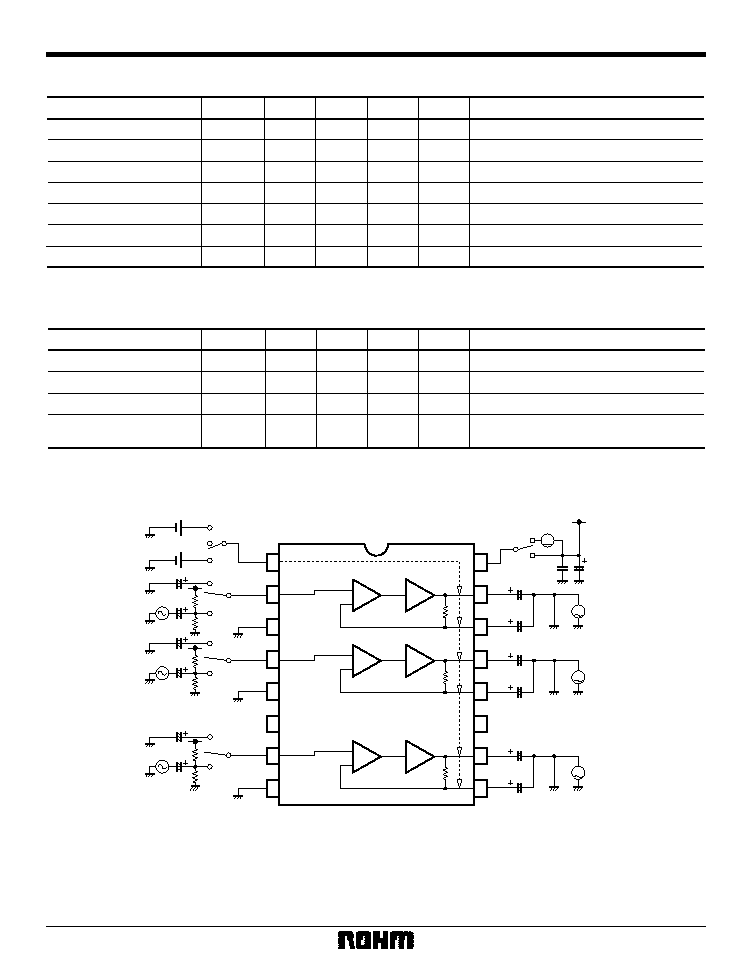
1
2
3
4
5
6
7
8
16
15
14
13
12
11
10
9
75
6dB
75
6dB
75
6dB
75
When the sag correction function is used.
6dB
Composite Video
D / A
D / A
D / A
Composite Y
N.C.
Chroma
MUTE
5V
N.C.
1000
µ
F
+
75
75
Vcc
0.1
µ
F
47
µ
F
+
1000
µ
F
+
75
75
75
1000
µ
F
+
75
75
75
100
µ
F
+
22
µ
F
+
∑
Application example
SSOP-A16
0.36
±
0.1
0.8
0.11
6.6
±
0.2
4.4
±
0.2
6.2
±
0.3
1.5
±
0.1
1
16
8
9
0.15
0.3Min.
0.15
±
0.1
∑
External dimensions (Units: mm)