 | –≠–ª–µ–∫—Ç—Ä–æ–Ω–Ω—ã–π –∫–æ–º–ø–æ–Ω–µ–Ω—Ç: BA7664FV | –°–∫–∞—á–∞—Ç—å:  PDF PDF  ZIP ZIP |
1
Multimedia ICs
75
driver with Y / C MIX circuit
BA7664FV
The BA7664FV is a 75
driver with a 6dB amplifier and a Y / C MIX circuit. The 75
driver is capable of driving a
load sufficient for two circuits, as well as being equipped with a sag correction function which reduces the capaci-
tance of the output coupling capacitor. The IC comes in the compact 8-pin SSOP-B package. The composite Y sig-
nal input pin is sync chip clamped input, while the chrominance input pin is bias input. An internal power-saving cir-
cuit is also included which provides an output muting function and output pin shorting protection.
∑
Applications
Video cameras, electronic cameras and others
∑
Features
1) The compact 8-pin SSOP-B package is used.
2) Operates at a low power consumption (60mW Typ.).
3) Internal Y / C MIX circuit.
4) Internal output muting circuit.
5) Internal power-saving circuit.
6) Internal output protection circuit.
7) Internal sag correction function makes it possible to
reduce the capacitance of the output coupling
capacitor.
8) A load sufficient for two circuits can be driven.
∑
Absolute maximum ratings (Ta = 25∞C)
Parameter
Symbol
Limits
Unit
Power supply voltage
Power dissipation
Operating temperature
Storage temperature
V
CC
Pd
T
opr
T
stg
8
350
≠ 25 ~ + 75
≠ 55 ~ + 125
V
mW
∞
C
∞
C
Reduced by 3.5mW for each increase in Ta of 1
∞
C over 25
∞
C
∑
Recommended operating conditions (Ta = 25∞C)
Parameter
Symbol
Unit
Max.
Typ.
Min.
Operating power supply voltage
V
CC
4.5
5.5
5.0
V
Not designed for radiation resistance.
2
Multimedia ICs
BA7664FV
∑
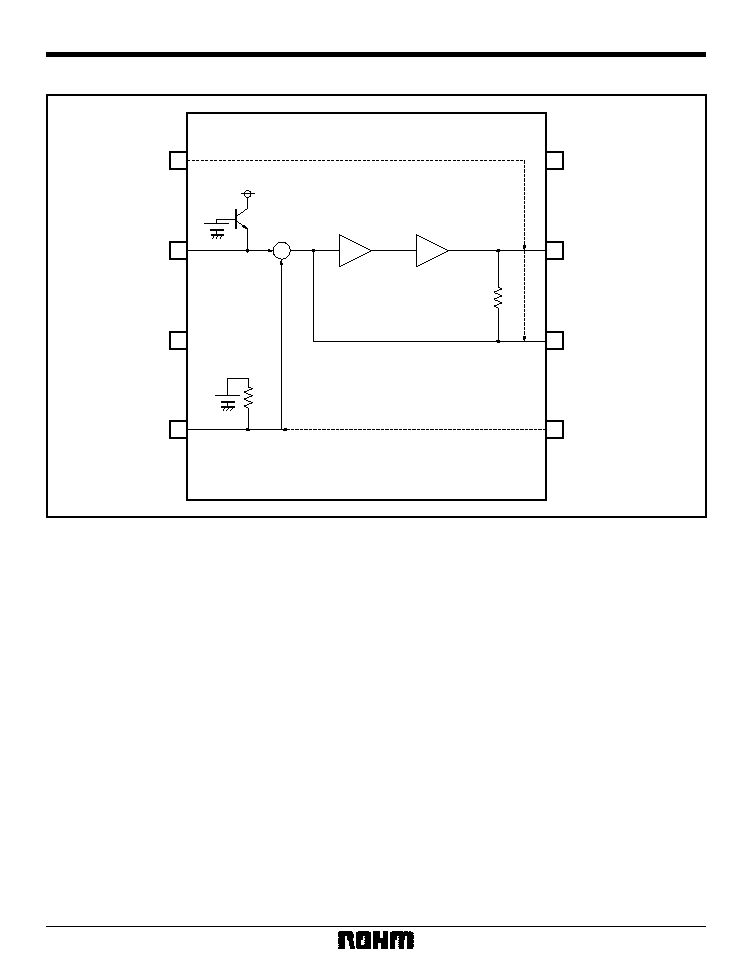
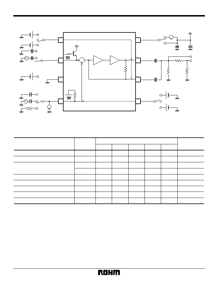
Block diagram
+
6dB
75
20k
MUTEA
1
Y
IN
2
GND
3
C
IN
4
V
CC
8
OUT1
7
OUT2
6
MUTEB
5
MUTE
CHROMA MUTE
3
Multimedia ICs
BA7664FV
∑
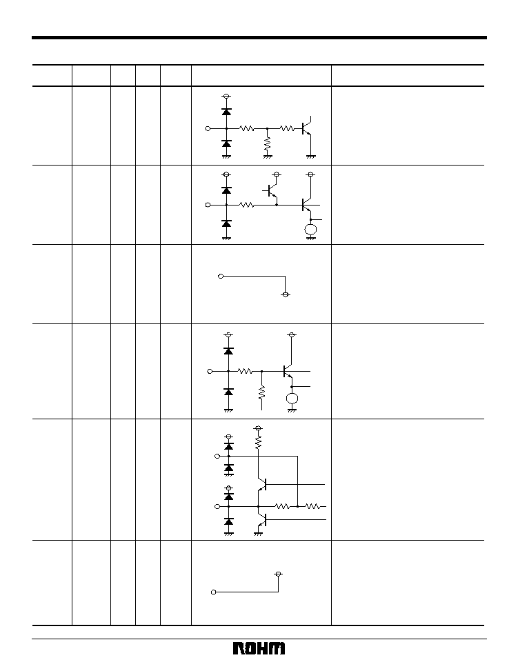
Pin descriptions and input / output circuits
Pin. No
Pin name
IN
OUT
Reference
potential
Equivalent circuit
Pin description
MUTEA
MUTEB
K
--
--
K
--
2.0V
--
--
0V
1
5
2
3
Y
IN
GND
Muting control
If MUTEA (pin 1) is set to HIGH, the
output is muted. If MUTEB (pin 8) is
set to HIGH, only the chrominance
signal is muted. (The Y signal is
output without being muted.)
Signal input
This is the input pin for composite Y
signals, and is sync chip clamped
input.
Ground
15k
14k
GND
4
C
IN
K
--
2.0V
--
K
0.9V
0.95V
6
7
MIXOUT2
MIXOUT1
--
--
5.0V
8
V
CC
Signal input
This is the input pin for chrominance
signals, and is bias-type input. The
input impedance is 20k
.
Signal output
These are the Y / C MIX signal output.
Pin 6 is the pin for sag correction. If
pin 7 is set to 0.2V or less, the
protective circuit is triggered and the
power-saving mode is accessed.
Power supply
6pin
20k
7pin
V
CC
4
Multimedia ICs
BA7664FV
∑
Electrical characteristics (unless otherwise noted, Ta = 25∞C, V
CC
= 5V)
Parameter
Symbol
Min.
Typ.
Max.
Unit
Conditions
Circuit current
Max. output level
Voltage gain
Frequency characteristic
Muting attenuation
Muting switching high level
Muting switching low level
Input impedance
Circuit current when muted
I
CC
V
om
G
V
G
F
M
T
V
THH
V
THL
Z
IN
I
MUTE
6.1
2.6
≠ 1.0
≠ 1.5
--
2.2
0
16
--
12.2
3.0
≠ 0.2
≠ 0.5
≠ 60
--
--
20
1.3
18.3
--
0.6
0.5
--
V
CC
0.7
24
2.6
mA
V
P-P
dB
dB
dB
V
V
k
mA
With no signal
f = 1kHz,THD = 1%V
02
f = 4.43MHz / V
01
f = 7MHz / 1MHz,1V
P-P
/ V
01
f = 4.43MHz,1V
P-P
/ V
01
--
--
Chrominance input pin (pin 7)
MUTEA "H"
∑
Guaranteed design parameters (unless otherwise noted, Ta = 25∞C, V
CC
= 5V)
Parameter
Symbol
Min.
Typ.
Max.
Unit
Conditions
Differential gain
Differential phase
DG
DP
--
--
1.0
0.5
2.0
2.0
%
DEG
V
IN
= 1.0V
P-P
reference staircase signal
V
IN
= 1.0V
P-P
reference staircase signal
∑
Mute switch mode settings
MUTE
∑ MUTEA (1pin)
H
NORMAL
L
CHROMA MUTE
∑ MUTEB (5pin)
H
NORMAL
L
5
Multimedia ICs
BA7664FV
∑
Measurement circuit
6dB
75
+
20k
1
2
3
4
8
7
6
5
MUTE
CHROMA MUTE
V
+
+
+
100
µ
22
µ
0.1
µ
V
02
V
01
47
µ
SW16
1
2
150
75
75
2.1V
0.8V
1
2
3
SW5
2.1V
0.8V
1
2
1
2
3
2.5V
3
SW1
SW2
+
+
1
µ
F
1
µ
F
1
2
3
0.1
µ
F
0.1
µ
F
SW4
A
Fig.1
∑
Measurement conditions
Parameter
Symbol
Measurement
method
SW Conditions
Circuit current
Max. output level
Voltage gain Y
OUT
C
OUT
Frequency characteristic
Muting attenuation
Chroma muting attenuation
Input impedance
Circuit current when muted
I
CC
V
OM
G
V1
G
V2
G
F
M
T
M
TC
Z
IN
I
MUTE
1
2
3
3
4
5
5
6
7
1
2
3
3
3
3
1
3
3
1
2
1
2
2
3
1
2
3
1
1
4
1
1
1
2
2
1
2
3
1
5
2
3
3
3
3
3
1
3
2
8
1
2
2
2
2
2
2
2
1
The muting switching level is substituted by carrying out the above measurement at H = 2.1V, L = 0.8V.
Measurement method
1 Measure the circuit current when no signal is present.
2 Apply a sine wave of f = 1kHz to the input, and adjust the input level so that the output distortion is 1%.
At this time, set the output voltage to the maximum output level of V
OM
[V
P-P
].
3 Measure the output V
O
[V
P-P
] with a sine wave of f = 4.43MHz, 1V
P-P
applied to the input.
Voltage gain G
V
is: G
V
= 20 Log (V
O
/ V
IN
) [dB]
4 Measure the outputs V
O7
and V
O1
[V
P-P
] each with sine waves of f = 7MHz, 1V
P-P
and f = 1MHz, 1V
P-P
applied to the input.
Voltage frequency G
F
is: G
F
= 20 Log (V
O7
/ V
O1
) [dB]
5 Measure the output V
O
[V
P-P
] with a sine wave of f = 4.43MHz, 1V
P-P
applied to the input.
The muting attenuation M
T
is: M
T
= 20 Log (V
O
/ V
IN
) [dB]
6 Measure the input voltage V
INSO
[V] and the open voltage of the input V
INO
[V] when 50
µ
A is introduced.
The input impedance Z
IN
is: Z
IN
= |V
INSO
≠ V
INO
| / 50
◊
1000 [k
]
7 Measure the circuit current when MUTEA (pin 1) is HIGH.