 | –≠–ª–µ–∫—Ç—Ä–æ–Ω–Ω—ã–π –∫–æ–º–ø–æ–Ω–µ–Ω—Ç: BA823 | –°–∫–∞—á–∞—Ç—å:  PDF PDF  ZIP ZIP |
1
Standard ICs
8-bit, serial IN, parallel OUT driver
BA823 / BA823F
The BA823 and BA823F are 8-bit serial input, parallel output drivers. These monolithic ICs were developed as
drivers for thermal printing heads, LED character displays, and other similar applications.
∑
Applications
Thermal printing head drivers
LED character display drivers
∑
Features
∑
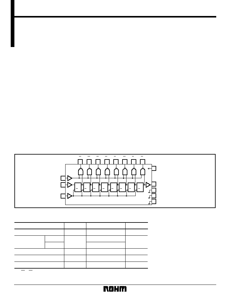
Block diagram
∑
Absolute maximum ratings (Ta = 25∞C)
1
15
2
3
13
4
14
S
D
I
C
12
11
10
9
8
7
6
5
O
0
O
1
O
2
O
3
O
4
O
5
O
6
O
7
16
V
CC
GND
1
GND
2
GND
(Dig)
D Q
C
D Q
C
D Q
C
D Q
C
D Q
C
D Q
C
D Q
C
D Q
C
STROBE INPUT
DATA INPUT
SHIFT PULSE
DATA OUTPUT Do
1) Can drive up to 200 mA.
2) Controlling the strobe terminal with the drive timing
pulse enables current to be reduced when drive is
not being carried out.
3) Using the data output terminal for the next data input
enables cascade connections.
4) The digital ground and power ground are separated.
5) TTL and CMOS drive possible.
Parameter
Symbol
Limits
Unit
V
CC
7.0
1
V
BA823
Pd
550
2
mW
BA823F
500
3
V
IN Max.
+ 0.3 ~ + 6.0
V
Topr
≠ 20 ~ + 75
∞
C
Tstg
≠ 55 ~ + 125
∞
C
Power supply voltage
Power dissipation
Input voltage
Operating temperature
Storage temperature
1 O
0
to O
7
output pins are 34V (max.).
2 Reduced by 5.5mW for each increase in Ta of 1
∞
C over 25
∞
C.
3 Reduced by 5mW for each increase in Ta of 1
∞
C over 25
∞
C.
2
Standard ICs
BA823 / BA823F
∑
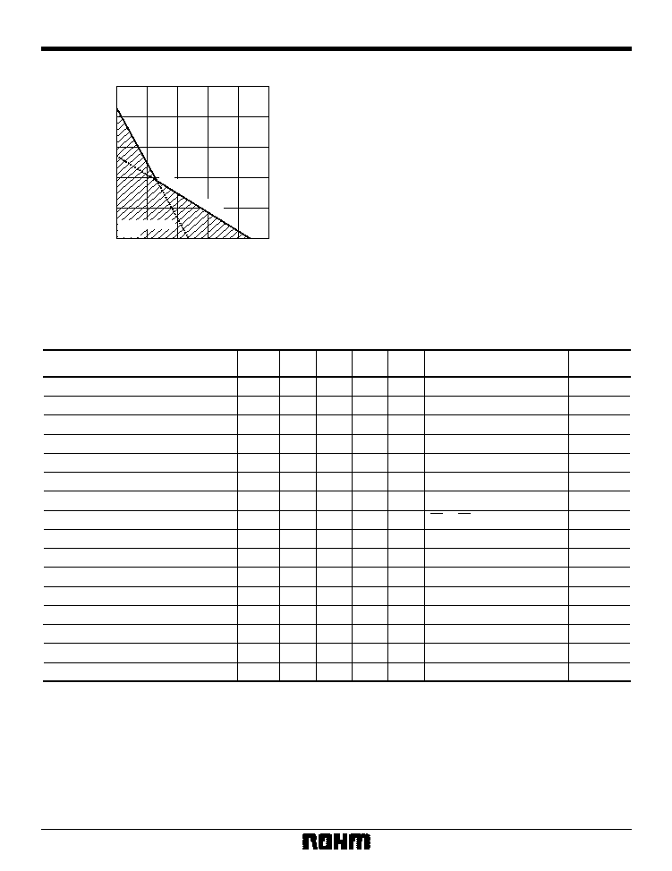
Usage conditions range
200
100
0
0
10
20
OUTPUT CURRENT : I
OUT
(mA)
SUPPLY VOLTAGE : V
CC
(V)
Fig. 1 Power supply voltage and output current
usage conditions (Per Circuit)
The maximum usage conditions, shown on the
left, indicate the absolute maximums for power
supply voltage and IC output current. Never
exceed these usage conditions, under any
circumstances.
Fig. 1 Power supply voltage and
output current usage conditions
Max. usage conditions
Usage conditions
range
∑
Electrical characteristics (unless otherwise noted, Ta = 25∞C, V
CC
= + 5.0V)
Parameter
Symbol
Min.
Typ.
Max.
Unit
Conditions
Measurement
circuit
V
CC
4.5
5.0
5.5
V
Fig.2
I
Q1
--
4
6
mA
Fig.2
I
Q2
--
8
11
mA
Fig.2
V
IL
--
--
0.8
V
Fig.2
V
IH
2
--
--
V
Fig.2
I
IH
--
--
0.4
mA
Fig.2
I
IH
--
--
100
µ
A
Fig.2
V
O OFF
--
--
21.8
V
Fig.3
V
O ON
--
0.8
1.3
V
Fig.3
I
OL
--
--
207
mA
Fig.3
V
DOH
2.4
--
--
V
Fig.3
V
DOL
--
--
0.8
V
Fig.3
t
1
--
--
300
ns
--
t
2
--
--
1
µ
s
--
t
3
--
--
1
µ
s
--
f
Max
.
500
--
--
kHz
--
Power supply voltage
Quiescent current 1
Quiescent current 2
Input low level voltage
Input high level voltage
Input high level current
Input high level current
Maximum output voltage
Output saturation voltage
Output current
"H" level data output voltage
"L" level data output voltage
Minimum setup time
Minimum shift pulse width
Minimum timing time
Maximum data transfer speed
--
--
R
L
= 10k
--
V
IH
= 2.0V, V
IL
= 0.8V
V
IH
= 2.0V, V
IL
= 0.8V
V
IH
= 2.0V, V
IL
= 0.8V
V
IH
= 2.0V, V
IL
= 0.8V
V
CC
pin
When all data values are "0"
When all data values are "0"
V
IN
= 4.5 V
V
IN
= 2.0 V
O
0
to O
7
pins, I
O
= 10
µ
A
When I
O
= 100mA sink
Applied voltage V = 11.8V
3
Standard ICs
BA823 / BA823F
∑
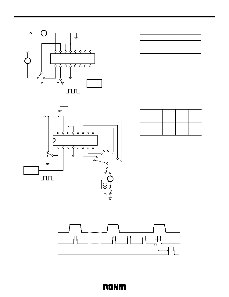
Measurement circuits
V
CC
= 5.0V
PG
1
1
3
2
2
SW
2
SW
1
V
IN
= 4.5V
BA823 / F
A
A
Data should be left at "0"
After 8 or more pulses have elapsed
Fig. 2 I
CC
and I
IH
measurement circuit
V
CC
= 5.0V
1
2
SW
1
SW
3
SW
2
100mA
82
V
A
I
O
2
1
8
7
6
5
4
3
2
1
BA823 / F
PG
A
After 8 or more pulses have elapsed
Fig. 3 V
O
ON
, V
O
OFF
and I
OL
measurement circuit
Item
I
CC
1
1
I
IH
2
1 ~ 3
SW
1
SW
2
Item
V
O ON
1
1 ~ 8
1
I
OL
1
1 ~ 8
2
V
O OFF
2
1 ~ 8
2
SW
1
SW
2
SW
3
When tested at V
O
OFF
: I
O
= 10
µ
A
When tested at I
O ON
: V
A
= 30V
∑
Input conditions
t
1
t
2
t
3
Fig. 4
Data input
D
1
Shift pulse
C
Print pulse
S
4
Standard ICs
BA823 / BA823F
∑
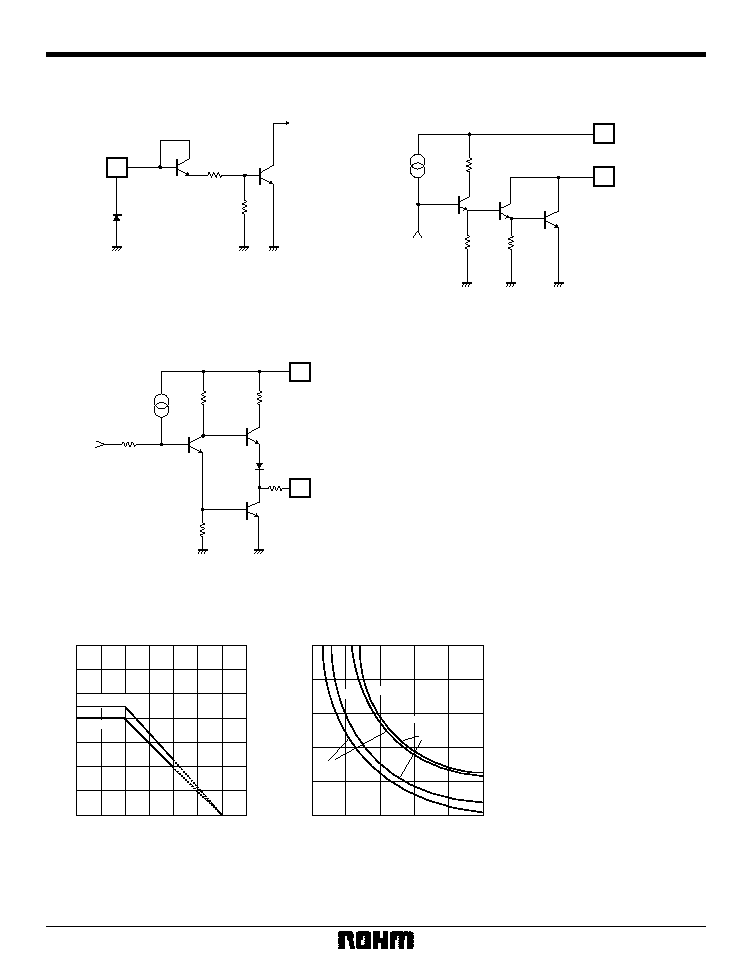
Input / output circuits
1, 2, 15pin
10k
20k
(a) Input circuit
10k
5k
100
500
3pin
V
CC
200
(c) Data output circuit
Fig.5
12k
1.0k
5.5k
V
CC
5, 6, 7, 8, 9, 10,
11, 12pin
(b) Output circuit
∑
Electrical characteristic curves
AMBIENT TEMPERATURE : Ta (
∞
C)
POWER DISSIPATION : Pd (mW)
750
500
250
0
≠ 25
0
25
50
75
100
BA823F
125
150
BA823
Fig. 6 Power dissipation vs.
ambient temperature
OUTPUT DUTY CYCLE (ALL BIT "ON") (%)
MAXIMUM OUTPUT CURENT : I
OM
(mA)
200
160
120
80
40
20
40
60
80
100
18mA
22mA
42mA
48mA
13%
30%
34%
15%
BA823
BA823F
Ta = 75
∞
C
Ta = 25
∞
C
At repetition frequency of 1 Hz or higher
Fig. 7 Output conditions
5
Standard ICs
BA823 / BA823F
∑
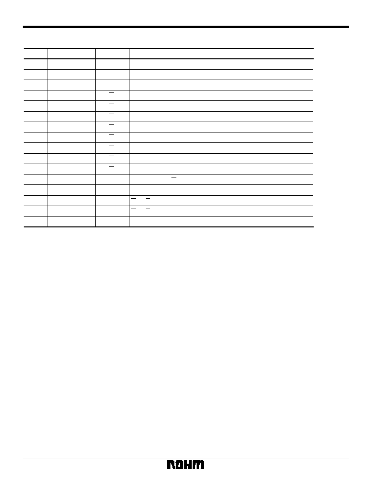
Pin descriptions
C
S
O
0
O
1
O
2
O
3
O
4
O
5
O
6
O
7
D
O
V
CC
GND
1
GND
2
D
I
GND (Dig)
2
15
1
12
11
10
9
8
7
6
5
3
16
13
4
14
Pin No.
SHIFT PULSE
DATA INPUT
STROBE
OUTPUT
OUTPUT
OUTPUT
OUTPUT
OUTPUT
OUTPUT
OUTPUT
OUTPUT
DATA OUTPUT
V
CC
GND
GND
GND
Pin name
Code
Function
Shift pulse of shift register
Data input of shift pulse registered using shift pulse rise
When "1", the content of the shift register is output
"0" when the content of the register is "1" on the 1st bit
"0" when the content of the register is "1" on the 2nd bit
"0" when the content of the register is "1" on the 3rd bit
"0" when the content of the register is "1" on the 4th bit
"0" when the content of the register is "1" on the 5th bit
"0" when the content of the register is "1" on the 6th bit
"0" when the content of the register is "1" on the 7th bit
"0" when the content of the register is "1" on the 8th bit
Has passed the O
7
output circuit and becomes the input for the next step
Normally 5.0V used (
±
10%)
O
0
to O
3
output circuit GND
O
4
to O
7
output circuit GND
Logic circuit GND