 | ÐлекÑÑоннÑй компоненÑ: BA8272AFV | СкаÑаÑÑ:  PDF PDF  ZIP ZIP |
Headphone driver for
BA8272AFV
Audio ICs
1/8
BUS Interface for car audio
BA8272AFV
BA8272AFV is a BUS interface IC (slave side) developed for car audio systems. Communication system of BUS ON,
DATA, CLOCK, and RESET can be constructed in combination with BA8270F / BA8270FV (master side). This IC can be
used for communication between the audio system and other applications such as power amplifier, CD, MD changer,
navigation and TV.
!
Applications
Car audio
!
Features
1) It can be used for 3V Interface system.
2) It can build up the communication system of BUS ON, DATA, CLOCK and RESET in combination with BA8270FV
(IC at a master side) in pairs.
3) Suitable for car audio.
!
!
!
!
Absolute maximum ratings (Ta=25
°C)
Parameter
Symbol
Limits
Unit
Supply voltage
V
V
Power dissipation
Pd
mW
Operating temperature range
Topr
°
C
Storage temperature range
Range of voltage applied to
an inter terminal
Tstg
-
°
C
Reduced by 4mW for each increase in Ta of 1
°
C over 25
°
C. (Board size 50
×
50
×
1.6mm)
The operating temperature range shall be within I
L
=
50mA.
V
CC
7.0
400
-
40~
+
85
-
55~
+
125
-
0.3~
+
7.0
!
!
!
!
Recommended operating conditions (Ta=25
°C)
Parameter
Symbol
Min.
Typ.
Max.
Unit
Supply voltage
2.8
-
7.0
V
V
CC
BA8272AFV
Audio ICs
2/8
!
!
!
!
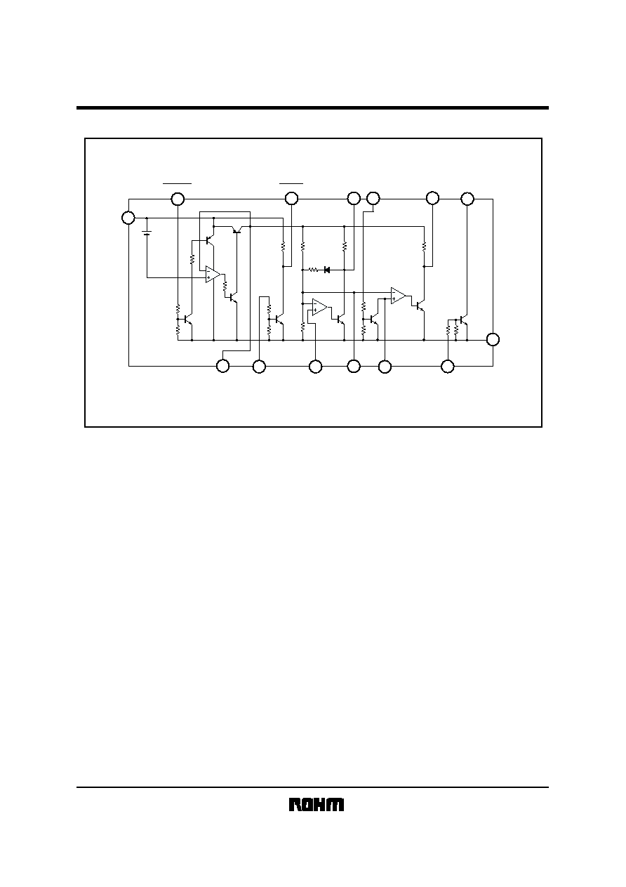
Block diagram
V
CC
LINK OFF
BUS ON
CLK OUT DATA IN
DATA OUT
RESET
BUS RESET
BUS CLK
BUS ON IN
BUS ON OUT
BUS DATA
VREF
GND
R23
47k
R22
1k
R21
4.7k
R16
4.7k
R14
22k
R3
47k
R2
47k
R10
47k
R9
26k
R5
3.9k
R32
27k
Q42
R26
12.3k
R24
19.7k
R1
26k
8
3
9
10
11
14
7
6
5
4
2
12
13
1
BA8272AFV
Audio ICs
3/8
!
!
!
!
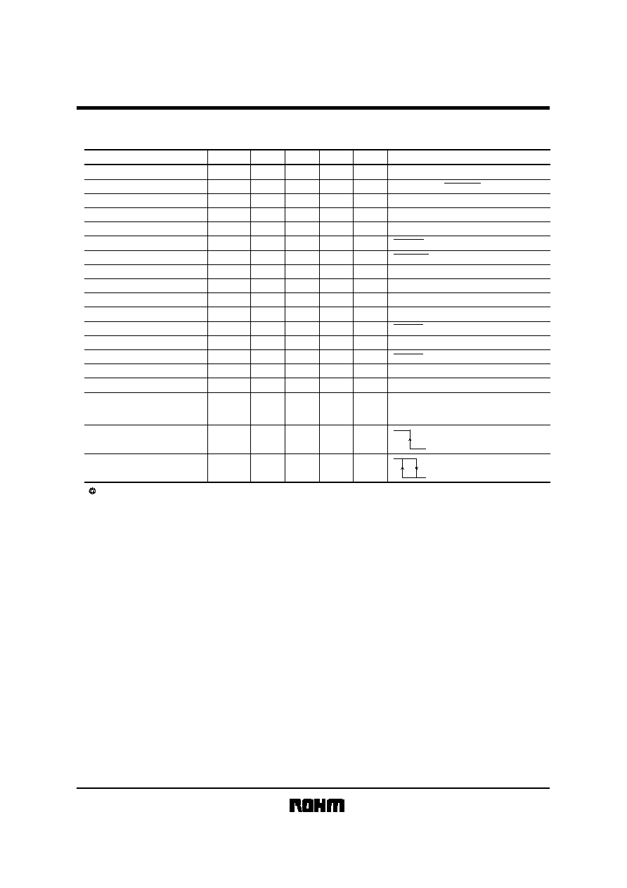
Electrical characteristics
_
(unless otherwise noted, Ta=25
°C, Vcc=5.5V)
Parameter
Symbol
Min.
Typ.
Max.
Unit
Conditions
Circuit current 1
I
CC
1
I
IN
1
I
IN
2
I
IN
3
I
IN
4
I
IN
5
I
IN
6
V
SAT
2
V
SAT
1
V
BON
V
HBA
V
TH
V
HYS
R3
R21
I
CC
2
I
CC
3
V
LOSS
1
V
LOSS
2
-
µ
A
µ
A
µ
A
µ
A
Circuit current 2
-
mA
Circuit current 3
-
-
-
-
-
-
mA
I
L
=
100mA
V
V
V
CC
-BUS ON OUT voltage 1
V
CC
-BUS ON OUT voltage 2
75
75
10
10
330
3.5
Input terminal current 1
Input terminal current 2
Input terminal current 3
Input terminal current 4
Input terminal current 5
Input terminal current 6
Output internal resistor 1
Output saturation voltage 1
Output saturation voltage 2
Reset output voltage
CLK OUT output "H" level
BUS CLK input threshold level
BUS CLK input hysteresis width
This product is not designed for protection against radio active rays.
Output internal resistor 2
µ
A
mA
k
k
V
V
V
V
V
mV
µ
A
35.2
3.52
0.75
300
VHI
-
0.3
-
1.1
5.0
0.15
0.09
0.2
0.1
0.2
100
100
25
25
395
4.8
47
4.7
0.80
400
VHI
-
0.5
10
3.0
13.0
0.35
0.2
0.4
0.25
0.4
140
140
40
40
500
6.4
58.8
5.88
0.85
500
VHI
-
0.7
Upon no load, all the terminals turn OFF.
I
L
=
50mA
BUS RESET terminal 5.5V input
DATA OUT terminal
BUS DATA pull up resistance 1k
0V inputted into the BUS CLOCK terminal.
"H" level of the BUS ON OUT terminal shall
be V
H1
. V
HBA
=
V
H1
-
V
H3
I
8
=
1mA, BUS RESET terminal 5.5V
CLK OUT terminal observation
I
L
=
40mA
BUS CLK terminal 5.5V input
BUS DATA terminal 5.5V input
DATA IN terminal 5.5V input
Upon no load LINK OFF
=
5.5V
BUS ON input terminal 5.5V input
BUS ON terminal
BUS ON, CLK OUT, DATA OUT
LINK OFF terminal 5.5V input
CLK OUT terminal observation
BA8272AFV
Audio ICs
4/8
!
!
!
!
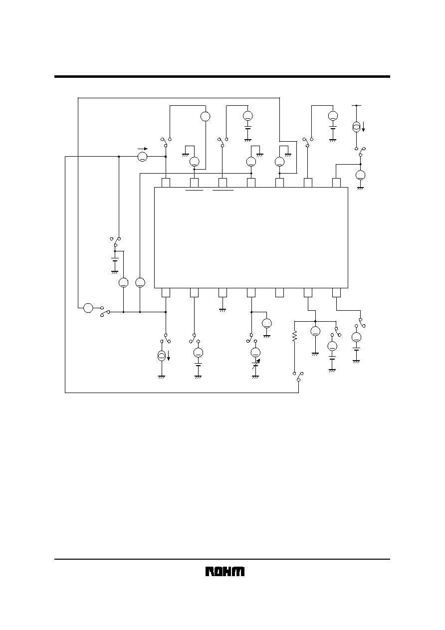
Measurement circuit
8
9
10
11
12
13
14
7
6
5
4
3
2
1
V
V
V
A
Fig.1
V
CC
LINK OFF
BUS ON
CLK OUT
DATA IN
DATA OUT
RESET
V8 on
V10
V11
5.5V
5.5V
5.5V
5.5V
5.5V
5.5V
0V
V6
R21
E2
E4
E6
E7
V13
R3
I
CC
V
CC
I
L
V
LOSS
V
HB
S7
S8
S9
E12
S10
S1
S2
S3
S4
1k
S5
S6
S12
S11
I8
E9
1
1
1
1
1
1
1
1
1
1
1
1
2
2
2
2
2
2
2
2
2
2
2
2
I
IN
5
I
IN
2
I
IN
1
I
IN
3
I
IN
6
I
IN
4
5.5V
1mA
+
+
+
+
+
+
+
+
+
+
+
+
+
+
+
BUS CLK
GND
BUS ON IN
BUS
ON OUT
BUS DATA
VREF
BUS
RESET
A
A
A
V
V
V
V
V
A
A
A
BA8272AFV
Audio ICs
5/8
SW operation table of measurement circuit diagram
Parameter
Symbol
S
1
S
2
S
3
S
4
S
5
S
6
S
7
S
8
S
9
S
10
S
11
S
12
Mesurement
terminal
Conditions
R3
R21
Pin14
Pin2
Pin12
Pin4
Pin14
Pin14
Pin1
-
Pin14
Pin1
-
Pin14
Pin9
Pin7
Pin13
-
Pin14
Pin1
-
Pin10
Pin13
Pin6
Pin10
Pin11
Pin8
Pin1
-
Pin11
Pin4
Pin4
Pin6
1
1
1
1
1
1
1
1
1
1
1
1
1
1
1
1
2
1
1
1
1
1
1
1
1
1
2
1
1
1
1
1
1
1
2
1
1
1
1
1
1
1
1
1
2
2
2
1
1
1
1
1
1
1
1
1
1
1
1
1
1
1
1
2
2
2
2
2
2
2
2
2
2
2
1
1
2
2
2
2
2
2
2
2
1
1
1
1
1
1
1
1
1
1
1
1
2
1
1
1
1
1
1
1
1
1
1
1
1
1
1
1
2
1
1
1
1
1
1
2
1
1
1
2
2
2
1
1
1
1
1
1
1
1
2
1
1
1
1
1
2
1
1
1
2
2
2
1
1
1
1
1
1
1
1
1
1
2
1
1
1
1
1
1
2
1
1
1
1
1
1
1
1
1
1
1
1
1
1
1
1
1
1
1
1
2
1
1
1
1
1
1
1
1
1
1
1
1
1
1
2
1
1
1
1
1
1
1
1
1
1
1
1
1
1
1
1
1
1
2
1
1
1
1
1
1
1
1
1
1
1
1
2
2
2
2
1
2
1
1
1
1
1
1
1
2
2
1
2
2
2
2
E
12
=
5.5V, I
L
=
100mA
E
12
=
5.5V, I
L
=
50mA
E
7
=
5.5V
E
9
=
5.5V, BUS DATA terminal
E
7
=
5.5V, RESET terminal
E
4
=
0V, E
12
=
5.5V
E
4
=0~3V, sweep, E
12
=
5.5V
E4=0~3V, sweep, E
12
=
5.5V
E
12
=
5.5V, I
L
=
40mA
E
4
=
5.5V
E
6
=
5.5V
E
9
=
5.5V
E
12
=
5.5V
E
2
=
5.5V
E
4
=
5.5V, CLK OUT terminal, E
12
=
5.5V
E
6
=
5.5V, DATA OUT terminal, E
12
=
5.5V
E
12
=
5.5V
E
2
=
5.5V, BUS ON terminal
Circuit current 1
V
SAT
2
V
SAT
1
V
SAT
1
V
SAT
1
V
BON
V
HBA
V
TH
V
HYS
I
CC
1
I
IN
1
I
IN
2
I
IN
3
I
IN
4
I
IN
5
I
IN
6
I
CC
2
I
CC
3
V
LOSS
1
V
LOSS
2
Circuit current 2
Circuit current 3
V
CC
-BUS ON OUT voltage 1
V
CC
-BUS ON OUT voltage 2
Input terminal current 1
Input terminal current 2
Input terminal current 3
Input terminal current 4
Input terminal current 5
Input terminal current 6
Output internal resistor 1
Output saturation voltage 1
Output saturation voltage 1
Output saturation voltage 1
Output saturation voltage 2
Reset output voltage
CLK OUT output "H" level
BUS CLK input threshold level
BUS CLK input hysteresis width
Output internal resistor 2
!
!
!
!
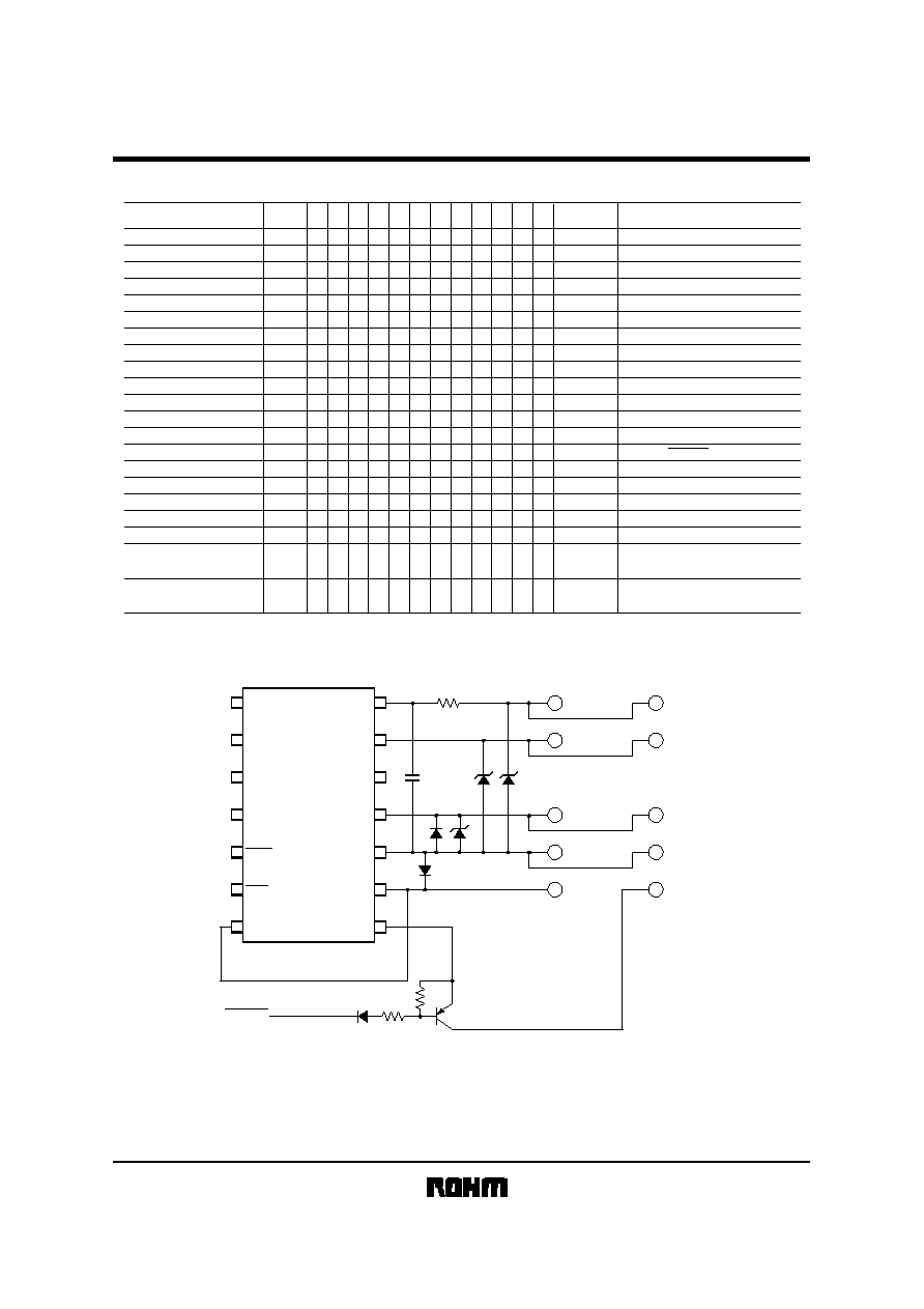
Application example
Fig.2
8
9
10
11
12
13
14
7
6
5
4
3
2
1
V
CC
LINK OFF
LINK OFF
RESET
BUS. DATA
BUS.DATA
BUS. CLK
BUS ON
BUS ON
BUS. CLK
GND
GND
RESET
Slave micon
·
Establish a protection circuit woth Schottky diode to prevent an error in operation due to noise of GND potential or less of
BUS ON and BUS CLK.
·
Establish a protection circuit with Zener diode to prevent over-voltage.
Schottky
To master unit
To next slave unit
BUS ON
CLK OUT
DATA IN
DATA OUT
RESET
BUS CLK
GND
BUS ON IN
BUS
ON OUT
BUS DATA
VREF
BUS
RESET
E
E
B
B
C
C
A
A
F
F
Document Outline