 | ÐлекÑÑоннÑй компоненÑ: BAXXST | СкаÑаÑÑ:  PDF PDF  ZIP ZIP |
BA((ST / BA((SFP series
BA
ST / BASFP series
Regulator ICs
1/11
Regulator, low drop-out type with ON/OFF
switch
BA
ST / BA
SFP series
The BA
ST and BASFP series are variable, fixed output low drop-out type voltage regulators with an ON/OFF
switch.
These regulators are used to provide a stabilized output voltage from a fluctuating DC input voltage.
Fixed output voltages are 3.3V, 5V, 6V(SFP), 7V, 8V, 9V, 10V(ST), 12V(ST). The maximum current capacity is 1 A for
each of the above voltages.
!
Application
Constant voltage power supply
!
!
!
!
Features
1) Built-in overvoltage protection circuit, overcurrent protection circuit and thermal shutdown circuit
2) TO220FP-5, TO252-5 standard packages can be accomodated in wide application.
3) 0
µA (design value) circuit current when switch is off
4) Richly diverse lineup.
5) Low minimum I/O voltage differential.
!
!
!
!
Product codes
Output voltage (V)
Product No.
Output voltage (V)
Product No.
Variable
BA00AST / ASFP
8.0
BA08ST / SFP
9.0
BA09ST / SFP
3.3
BA033ST / SFP
10.0
BA10ST
5.0
BA05ST / SFP
12.0
BA12ST
6.0
BA06SFP
7.0
BA07ST / SFP
!
!
!
!
Absolute maximum ratings (Ta=25
°C)
Parameter
Symbol
Limits
Unit
Power supply voltage
V
CC
35
V
Power dissipation
Pd
2000
*1
TO220FP-5
TO252-5
1000
*2
mW
Operating temperature
Topr
-40~+85
°C
Storage temperature
Tstg
-55~+150
°C
Peak applied voltage
Vsurge
50
*3
V
*1 Reduced by 16mW for each increase in Ta of 1°C over 25°C.
*2 Reduced by 8mW for each increase in Ta of 1°C over 25°C.
*3 Voltage application time : 200 msec. or less
BA
ST / BASFP series
Regulator ICs
2/11
!
!
!
!
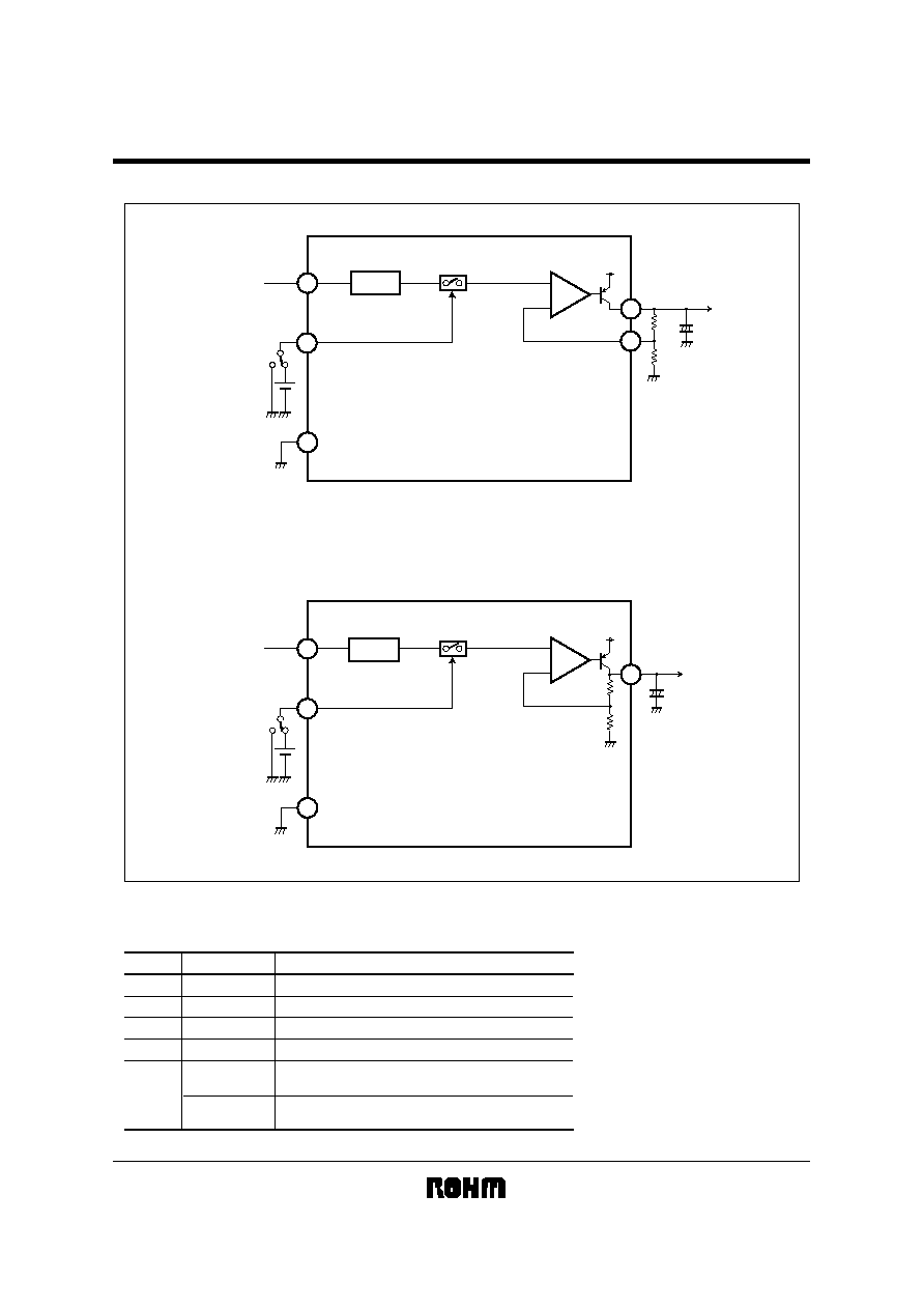
Block diagram
4
5
2
3
1
OUT
-
+
REFERENCE
VOLTAGE
GND
V
CC
CTL
C
4
2
3
1
OUT
-
+
+
+
GND
V
CC
CTL
Variable output type (BA00AST / ASFP)
Fixed output type
REFERENCE
VOLTAGE
!
!
!
!
Pin descriptions
Pin name
1
CTL
Output ON/OFF
2
V
CC
3
GND
4
OUT
5
C
N.C.
Power supply input
Ground
Output
Pin No.
Function
Reference power supply pin for setting voltage with
the BA00AST/ASFP.
In the BAOOST/SFP Series, these are NC pins,
except for the BA00AST/ASFP.
BA
ST / BASFP series
Regulator ICs
3/11
!
!
!
!
Recommended operating conditions
BA00AST / ASFP BA08ST / SFP
Parameter
Symbol
Min.
Max.
Unit
Input voltage
25
V
-
1
A
4
Output current
V
CC
I
O
Parameter
Symbol
Min.
Max.
Unit
9
25
V
-
1
A
V
CC
I
O
Input voltage
Output current
BA033ST / SFP BA09ST / SFP
Parameter
Symbol
Min.
Max.
Unit
4.3
25
V
-
1
A
V
CC
I
O
Input voltage
Output current
Parameter
Symbol
Min.
Max.
Unit
10
25
V
-
1
A
V
CC
I
O
Input voltage
Output current
BA05ST / SFP BA10ST
Parameter
Symbol
Min.
Max.
Unit
6
25
V
-
1
A
V
CC
I
O
Input voltage
Output current
Parameter
Symbol
Min.
Max.
Unit
11
25
V
-
1
A
V
CC
I
O
Input voltage
Output current
BA06SFP BA12ST
Parameter
Symbol
Min.
Max.
Unit
7
25
V
-
1
A
V
CC
I
O
Input voltage
Output current
Parameter
Symbol
Min.
Max.
Unit
13
25
V
-
1
A
V
CC
I
O
Input voltage
Output current
BA07ST / SFP
Parameter
Symbol
Min.
Max.
Unit
8
V
-
1
A
25
V
CC
I
O
Input voltage
Output current
!
!
!
!
Electrical characteristics
BA00AST / ASFP (unless otherwise noted, Ta=25
°C, Vcc=10V, Io=500mA)
Parameter
Symbol
Min.
Typ.
Max.
Unit
Conditions
Measurement
circuit
Reference voltage
Power save current
Output voltage
Input stability
Ripple rejection ratio
Load regulation
Temperature coefficient of output voltage
Minimum I/O voltage differential
Bias current
Peak output current
Output short-circuit current
ON mode voltage
OFF mode voltage
Input high level current
V
ref
1.200
1.225
1.250
V
Fig.1
V
O
-
5.0
-
V
Fig.1
Reg.I
-
20
100
mV
Fig.1
R.R.
45
55
-
dB
e
IN
=1Vrms, f=120Hz, I
O
=100mA
Fig.2
Reg.L
-
50
150
mV
I
O
=5mA
1A
Fig.1
T
CVO
-
±0.01
-
% / °C
I
O
=5mA, Tj=0~125°C
Fig.1
V
d
-
0.3
0.5
V
Fig.3
I
b
-
2.5
5.0
mA
I
O
=0mA
Fig.4
I
O
1.0
1.5
-
A
Tj=25°C
Fig.1
I
OS
-
0.4
-
A
V
CC
=25V
V
CC
=0.95V
O
Ist
-
0
10
µ
A
Fig.4
OFF mode
Fig.5
Vth1
2.0
-
-
V
Output Active mode, I
O
=0mA
Fig.6
Vth2
-
-
0.8
V
Output OFF mode, I
O
=0mA
Fig.6
I
IN
100
200
300
µ
A
CTL=5V, I
O
=0mA
Fig.6
V
CC
=6
25V
BA
ST / BASFP series
Regulator ICs
4/11
BA033ST / SFP (unless otherwise noted, Ta=25
°C, Vcc=8 V, Io=500 mA)
Parameter
Symbol
Min.
Typ.
Max.
Unit
Conditions
Measurement
circuit
Power save current
Output voltage
Input stability
Ripple rejection ratio
Load regulation
Temperature coefficient of output voltage
Minimum I/O voltage differential
Bias current
Peak output current
Output short-circuit current
ON mode voltage
OFF mode voltage
Input high level current
V
O1
3.13
3.3
3.47
V
Fig.1
Reg.I
-
20
100
mV
Fig.1
R.R.
45
55
-
dB
e
IN
=1Vrms, f=120Hz, I
O
=100mA
Fig.2
Reg.L
-
50
150
mV
I
O
=5mA
1A
Fig.1
T
CVO
-
±
0.02
-
% / °C
I
O
=5mA, Tj=0~125°C
Fig.1
V
d
-
0.3
0.5
V
V
CC
=0.95V
O
Fig.3
I
b
-
2.5
5.0
mA
I
O
=0mA
Fig.4
1.0
1.5
-
A
Tj=25°C
Fig.1
I
OS
-
0.4
-
A
V
CC
=25V
Fig.5
Vth1
2.0
-
-
V
Output Active mode, I
O
=0mA
Fig.6
Vth2
-
-
0.8
V
Output OFF mode, I
O
=0mA
Fig.6
I
IN
100
200
300
µ
A
CTL=5V, I
O
=0mA
Fig.6
V
CC
=4=.3
25V
I
ST
-
0
10
µ
A
Fig.4
OFF mode
I
O
BA05ST / SFP (unless otherwise noted, Ta=25
°C, Vcc=10 V, Io=500 mA)
Parameter
Symbol
Min.
Typ.
Max.
Unit
Conditions
Measurement
circuit
V
O1
4.75
5.0
5.25
V
Fig.1
Reg.I
-
20
100
mV
Fig.1
R.R.
45
55
-
dB
e
IN
=1Vrms, f=120Hz, I
O
=100mA
Fig.2
Reg.L
-
50
150
mV
I
O
=5mA
1A
Fig.1
T
CVO
-
±
0.02
-
% / °C
I
O
=5mA, Tj=0~125°C
Fig.1
V
d
-
0.3
0.5
V
V
CC
=4.75V
Fig.3
I
b
-
2.5
5.0
mA
I
O
=0mA
Fig.4
1.0
1.5
-
A
Tj=25°C
Fig.1
I
OS
-
0.4
-
A
V
CC
=25V
Fig.5
Vth1
2.0
-
-
V
Output Active mode, I
O
=0mA
Fig.6
Vth2
-
-
0.8
V
Output OFF mode, I
O
=0mA
Fig.6
I
IN
100
200
300
µ
A
CTL=5V, I
O
=0mA
Fig.6
V
CC
=6
2=5V
Power save current
Output voltage
Input stability
Ripple rejection ratio
Load regulation
Temperature coefficient of output voltage
Minimum I/O voltage differential
Bias current
Peak output current
Output short-circuit current
ON mode voltage
OFF mode voltage
Input high level current
I
ST
-
0
10
µ
A
Fig.4
OFF mode
I
O
BA06SFP ( unless otherwise noted, Ta=25
°C, Vcc=11 V, Io=500 mA)
Parameter
Symbol
Min.
Typ.
Max.
Unit
Conditions
Measurement
circuit
V
O1
5.7
6.0
6.3
V
Fig.1
Reg.I
-
20
100
mV
Fig.1
R.R.
45
55
-
dB
e
IN
=1Vrms, f=120Hz, I
O
=100mA
Fig.2
Reg.L
-
50
150
mV
I
O
=5mA
1A
Fig.1
T
CVO
-
±0.02
-
% / °C
I
O
=5mA, Tj=0
~125°C
Fig.1
V
d
-
0.3
0.5
V
V
CC
=5.7V
Fig.3
I
b
-
2.5
5.0
mA
I
O
=0mA
Fig.4
I
O
1.0
1.5
-
A
Tj=25
°C
Fig.1
I
OS
-
0.4
-
A
V
CC
=25V
Fig.5
Vth1
2.0
-
-
V
Output Active mode, I
O
=0mA
Fig.6
Vth2
-
-
0.8
V
Output OFF mode, I
O
=0mA
Fig.6
I
IN
100
200
300
µ
A
CTL=5V, I
O
=0mA
Fig.6
V
CC
=7
25V
Power save current
Output voltage
Input stability
Ripple rejection ratio
Load regulation
Temperature coefficient of output voltage
Minimum I/O voltage differential
Bias current
Peak output current
Output short-circuit current
ON mode voltage
OFF mode voltage
Input high level current
I
ST
-
0
10
µ
A
Fig.4
OFF mode
BA
ST / BASFP series
Regulator ICs
5/11
BA07ST / SFP (unless otherwise noted, Ta=25
°C, Vcc=12 V, Io=500 mA) (under development)
Parameter
Symbol
Min.
Typ.
Max.
Unit
Conditions
Measurement
circuit
V
O1
6.65
7.0
7.35
V
Fig.1
Reg.I
-
20
100
mV
Fig.1
R.R.
45
55
-
dB
e
IN
=1Vrms, f=120Hz, I
O
=100mA
Fig.2
Reg.L
-
50
150
mV
I
O
=5mA
1A
Fig.1
T
CVO
-
±0.02
-
% / °C
I
O
=5mA, Tj=0~125°C
Fig.1
V
d
-
0.3
0.5
V
V
CC
=6.65V
Fig.3
I
b
-
2.5
5.0
mA
I
O
=0mA
Fig.4
I
O
1.0
1.5
-
A
Tj
=25°C
Fig.1
I
OS
-
0.4
-
A
V
CC
=25V
Fig.5
Vth1
2.0
-
-
V
Output Active mode, I
O
=0mA
Fig.6
Vth2
-
-
0.8
V
Output OFF mode, I
O
=0mA
Fig.6
I
IN
100
200
300
µ
A
CTL
=5V, I
O
=0mA
Fig.6
V
CC
=8
25V
Power save current
Output voltage
Input stability
Ripple rejection ratio
Load regulation
Temperature coefficient of output voltage
Minimum I/O voltage differential
Bias current
Peak output current
Output short-circuit current
ON mode voltage
OFF mode voltage
Input high level current
I
ST
-
0
10
µ
A
Fig.4
OFF mode
BA08ST / SFP (unless otherwise noted, Ta=25
°C, Vcc=13 V, Io=500 mA)
Parameter
Symbol
Min.
Typ.
Max.
Unit
Conditions
Measurement
circuit
V
O1
7.6
8.0
8.4
V
Fig.1
Fig.4
Reg.I
-
20
100
mV
Fig.1
R.R.
45
55
-
dB
e
IN
=1Vrms, f=120Hz, I
O
=100mA
Fig.2
Reg.L
-
50
150
mV
I
O
=5mA
1A
Fig.1
T
CVO
-
±0.02
-
% / °C
I
O
=5mA, Tj=0
~125°C
Fig.1
V
d
-
0.3
0.5
V
V
CC
=0.95V
O
Fig.3
I
b
-
2.5
5.0
mA
I
O
=0mA
Fig.4
I
O
1.0
1.5
-
A
Tj=25
°C
Fig.1
I
OS
-
0.4
-
A
V
CC
=25V
Fig.5
Vth1
2.0
-
-
V
Output Active mode, I
O
=0mA
Fig.6
Vth2
-
-
0.8
V
Output OFF mode, I
O
=0mA
Fig.6
I
IN
100
200
300
µ
A
CTL=5V, I
O
=0mA
Fig.6
V
CC
9
25V
Power save current
Output voltage
Input stability
Ripple rejection ratio
Load regulation
Temperature coefficient of output voltage
Minimum I/O voltage differential
Bias current
Peak output current
Output short-circuit current
ON mode voltage
OFF mode voltage
Input high level current
I
ST
-
0
10
µ
A
OFF mode
BA09ST / SFP (unless otherwise noted, Ta=25
°C, Vcc=14 V, Io=500 mA)
Parameter
Symbol
Min.
Typ.
Max.
Unit
Conditions
Measurement
circuit
V
O1
8.55
9.0
9.45
V
Fig.1
Reg.I
-
20
100
mV
Fig.1
R.R.
45
55
-
dB
e
IN
=1Vrms, f=120Hz, I
O
=100mA
Fig.2
Reg.L
-
50
150
mV
I
O
=5mA
1A
Fig.1
T
CVO
-
±0.02
-
% / °C
I
O
=5mA, Tj=0~125°C
Fig.1
V
d
-
0.3
0.5
V
V
CC
=0.95V
O
Fig.3
I
b
-
2.5
5.0
mA
I
O
=0mA
Fig.4
I
O
1.0
1.5
-
A
Tj
=25°C
Fig.1
I
OS
-
0.4
-
A
V
CC
=25V
Fig.5
Vth1
2.0
-
-
V
Output Active mode, I
O
=0mA
Fig.6
Vth2
-
-
0.8
V
Output OFF mode, I
O
=0mA
Fig.6
I
IN
100
200
300
µ
A
CTL
=5V, I
O
=0mA
Fig.6
V
CC
=10
25V
Power save current
Output voltage
Input stability
Ripple rejection ratio
Load regulation
Temperature coefficient of output voltage
Minimum I/O voltage differential
Bias current
Peak output current
Output short-circuit current
ON mode voltage
OFF mode voltage
Input high level current
I
ST
-
0
10
µ
A
Fig.4
OFF mode
Document Outline