 | –≠–ª–µ–∫—Ç—Ä–æ–Ω–Ω—ã–π –∫–æ–º–ø–æ–Ω–µ–Ω—Ç: BD5260PW | –°–∫–∞—á–∞—Ç—å:  PDF PDF  ZIP ZIP |

Features
Applications
CMOS VOLTAGE DETECTOR IC
with Delay Time Circuit
BD52XXG/FVE
BD53XXG/FVE
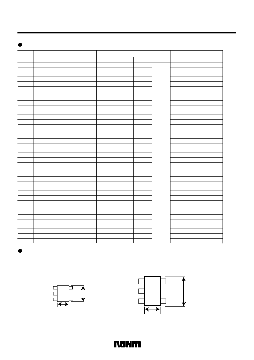
Selection guide
ROHM's BD52XXG/FVE and BD53XXG/FVE are series of high-accuracy, low-power VOLTAGE DETECTOR ICs
with a CMOS process. These series can set delay time by external capacitor. For flexible choice according to the
application, BD52XXG/FVE series with N channel open drain output and BD53XXG/FVE series with CMOS output
are available in 38 voltage types which detection voltage is from 2.3V to 6.0V in steps of 0.1V in different packages,
totaling 152 models.
1) Detection voltage: 0.1V step line-up 2.3~6.0V (Typ.)
2) High-accuracy detection voltage:
±1.5% guranteed (Ability ±1%)
3) Ultra low current consumption: 0.85
µA typ. (Output is High.)
4) Delay time can be set by external capacitor.
5) Nch open drain output (BD52XXG/FVE series), CMOS output (BD53XXG/FVE series)
6) Small package of VSOF5
(EMP5)
(BD52XXFVE/BD53XXFVE), and SSOP5
(SMP5C2)
(BD52XXG/BD53XXG)
Every kind of appliances with microcontroller and logic circuit
For BD5XXXX series, detection voltage, output circuit types (Refer to the block diagram at P3),and package
(Refer to the block diagram at P14) can be selected for your own application.Part number of devices for each
specification is shown below.
Part No. : B D 5 X X X X
Part No.
Specification
Contents
Output circuit types
Package
Detection voltage
2 : Open drain output
3 : CMOS output
Ex. : V
DET
: described in each 0.1V step
for 2.3V~6.0V range (29 means 2.9V)
G : SSOP5
(SMP5C2)
FVE : VSOF5
(EMP5)
1
2
3
1
2
3
1/15
Voltage detectors
BD52XXG/FVE
BD53XXG/FVE
Line-up
Pin layout
Nch Open drain output
( BD52XXG/FVE )
CMOS output
( BD53XXG/FVE )
Detection voltage V
DET
( V ) Ta=25∞C
Detection
voltage
V
DET
Hysteresis
voltage
( V,Typ. )
Package
Min.
Typ.
Max.
V
DET
X 0.05
5.9V
5.8V
5.7V
5.6V
5.5V
5.4V
5.3V
5.2V
5.1V
5.0V
4.9V
4.8V
4.7V
4.6V
4.5V
4.4V
4.3V
4.2V
4.1V
4.0V
3.9V
3.8V
3.7V
3.6V
3.5V
3.4V
3.3V
3.2V
3.1V
3.0V
2.9V
2.8V
2.7V
2.6V
2.5V
2.4V
2.3V
BD5259G/FVE
BD5258G/FVE
BD5257G/FVE
BD5256G/FVE
BD5255G/FVE
BD5254G/FVE
BD5253G/FVE
BD5252G/FVE
BD5251G/FVE
BD5250G/FVE
BD5249G/FVE
BD5248G/FVE
BD5247G/FVE
BD5246G/FVE
BD5245G/FVE
BD5244G/FVE
BD5243G/FVE
BD5242G/FVE
BD5241G/FVE
BD5240G/FVE
BD5239G/FVE
BD5238G/FVE
BD5237G/FVE
BD5236G/FVE
BD5235G/FVE
BD5234G/FVE
BD5233G/FVE
BD5232G/FVE
BD5231G/FVE
BD5230G/FVE
BD5229G/FVE
BD5228G/FVE
BD5227G/FVE
BD5226G/FVE
BD5225G/FVE
BD5224G/FVE
BD5223G/FVE
BD5359G/FVE
BD5358G/FVE
BD5357G/FVE
BD5356G/FVE
BD5355G/FVE
BD5354G/FVE
BD5353G/FVE
BD5352G/FVE
BD5351G/FVE
BD5350G/FVE
BD5349G/FVE
BD5348G/FVE
BD5347G/FVE
BD5346G/FVE
BD5345G/FVE
BD5344G/FVE
BD5343G/FVE
BD5342G/FVE
BD5341G/FVE
BD5340G/FVE
BD5339G/FVE
BD5338G/FVE
BD5337G/FVE
BD5336G/FVE
BD5335G/FVE
BD5334G/FVE
BD5333G/FVE
BD5332G/FVE
BD5331G/FVE
BD5330G/FVE
BD5329G/FVE
BD5328G/FVE
BD5327G/FVE
BD5326G/FVE
BD5325G/FVE
BD5324G/FVE
BD5323G/FVE
5.812
5.713
5.615
5.516
5.418
5.319
5.221
5.122
5.024
4.925
4.827
4.728
4.630
4.531
4.433
4.334
4.236
4.137
4.039
3.940
3.842
3.743
3.645
3.546
3.448
3.349
3.251
3.152
3.054
2.955
2.857
2.758
2.660
2.561
2.463
2.364
2.266
5.900
5.800
5.700
5.600
5.500
5.400
5.300
5.200
5.100
5.000
4.900
4.800
4.700
4.600
4.500
4.400
4.300
4.200
4.100
4.000
3.900
3.800
3.700
3.600
3.500
3.400
3.300
3.200
3.100
3.000
2.900
2.800
2.700
2.600
2.500
2.400
2.300
5.989
5.887
5.786
5.684
5.583
5.481
5.380
5.278
5.177
5.075
4.974
4.872
4.771
4.669
4.568
4.466
4.365
4.263
4.162
4.060
3.959
3.857
3.756
3.654
3.553
3.451
3.350
3.248
3.147
3.045
2.944
2.842
2.741
2.639
2.538
2.436
2.335
SSOP5
(SMP5C2)
/ VSOF5
(EMP5)
SSOP5
(SMP5C2)
/ VSOF5
(EMP5)
SSOP5
(SMP5C2)
/ VSOF5
(EMP5)
SSOP5
(SMP5C2)
/ VSOF5
(EMP5)
SSOP5
(SMP5C2)
/ VSOF5
(EMP5)
SSOP5
(SMP5C2)
/ VSOF5
(EMP5)
SSOP5
(SMP5C2)
/ VSOF5
(EMP5)
SSOP5
(SMP5C2)
/ VSOF5
(EMP5)
SSOP5
(SMP5C2)
/ VSOF5
(EMP5)
SSOP5
(SMP5C2)
/ VSOF5
(EMP5)
SSOP5
(SMP5C2)
/ VSOF5
(EMP5)
SSOP5
(SMP5C2)
/ VSOF5
(EMP5)
SSOP5
(SMP5C2)
/ VSOF5
(EMP5)
SSOP5
(SMP5C2)
/ VSOF5
(EMP5)
SSOP5
(SMP5C2)
/ VSOF5
(EMP5)
SSOP5
(SMP5C2)
/ VSOF5
(EMP5)
SSOP5
(SMP5C2)
/ VSOF5
(EMP5)
SSOP5
(SMP5C2)
/ VSOF5
(EMP5)
SSOP5
(SMP5C2)
/ VSOF5
(EMP5)
SSOP5
(SMP5C2)
/ VSOF5
(EMP5)
SSOP5
(SMP5C2)
/ VSOF5
(EMP5)
SSOP5
(SMP5C2)
/ VSOF5
(EMP5)
SSOP5
(SMP5C2)
/ VSOF5
(EMP5)
SSOP5
(SMP5C2)
/ VSOF5
(EMP5)
SSOP5
(SMP5C2)
/ VSOF5
(EMP5)
SSOP5
(SMP5C2)
/ VSOF5
(EMP5)
SSOP5
(SMP5C2)
/ VSOF5
(EMP5)
SSOP5
(SMP5C2)
/ VSOF5
(EMP5)
SSOP5
(SMP5C2)
/ VSOF5
(EMP5)
SSOP5
(SMP5C2)
/ VSOF5
(EMP5)
SSOP5
(SMP5C2)
/ VSOF5
(EMP5)
SSOP5
(SMP5C2)
/ VSOF5
(EMP5)
SSOP5
(SMP5C2)
/ VSOF5
(EMP5)
SSOP5
(SMP5C2)
/ VSOF5
(EMP5)
SSOP5
(SMP5C2)
/ VSOF5
(EMP5)
SSOP5
(SMP5C2)
/ VSOF5
(EMP5)
SSOP5
(SMP5C2)
/ VSOF5
(EMP5)
SSOP5
(SMP5C2)
/ VSOF5
(EMP5)
6.0V
BD5260G/FVE
BD5360G/FVE
5.910
6.000
6.090
Pin layout of VSOF5
(EMP5)
and SSOP5
(SMP5C2)
is different as shown below. (Fig.1, Fig.2)
When used as replacement, please consider the difference. (The detail of packages is shown at P14.)
(Note) Connect SUB pin with GND pin.
Fig.1
Fig.2
1
V
OUT
C.T.
2
V
DD
3
GND
5
4 N.C.
BD52XXG/BD53XXG
2.9mm
1.6mm
SSOP5
(SMP5C2)
Package
1
V
OUT
V
DD
2
SUB
3
N.C.
GND
5
4
BD52XXFVE/BD53XXFVE
1.6mm
1.2mm
VSOF5
(EMP5)
Package
2/15
Voltage detectors
BD52XXG/FVE
BD53XXG/FVE
To prevent the functional deterioration or thermal damage of semiconductor devices and ensure their service life
and reliability, they must be designed and reviewed in such a way that the absolute maximum rating can not be
exceeded in any cases or even at any moment.
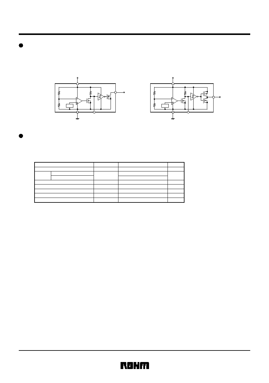
Two output types can be used. One is BD52XXG/FVE (Left) of open drain output type, and the other is
BD53XXG/FVE (Right) of CMOS output type.
∑ Operating temperature range
The circuit function is guaranteed within the temperature range. However, the operating characteristics are
different from that of Ta=25∞C. If they are any questions about the extent of guarantee of circuit functions
in this operating temperature range, please ask for more technical information.
∑ Output voltage
V
OUT
pin voltage should not exceed the indicated value. For Nch open drain output type, V
DD
applied
voltage and V
OUT
pin H output voltage can be used independently. Both of them should not exceed the
each indicated value.
∑ Power supply voltage
This voltage is the applied voltage between V
DD
and GND. The applied voltage should not exceed
the indicated value.
∑ Storage temperature range
This IC can be stored up to this temperature range without deterioration of characteristics. However, an
abrupt thermal shock of extreme temperature fluctuations may cause the deterioration of characteristics.
Output
voltage
Nch Open drain output
CMOS output
Power dissipation
SSOP5
(SMP5C2)
Power dissipation
VSOF5
(EMP5)
Operating temperature
Parameter
Symbol
Unit
V
OUT
Pd
Pd
T
opr
V
mW
mW
Storage temperature
T
stg
Limits
≠ 40 ~ + 85
≠ 55 ~ + 125
150
100
GND ≠ 0.3 ~ + 10
GND ≠ 0.3 ~ V
DD
+ 0.3
∞C
∞C
Power supply voltage
V
DD
≠ GND
≠ 0.3 ~ + 10
V
*
1
*
3
*
2
*
3
*
1 Derating : 1.5mW/∞C for operation above Ta=25∞C
*
2 Derating : 1.0mW/∞C for operation above Ta=25∞C
*
3 When only IC is used.
BD52XXG/FVE : Open drain output
BD53XXG/FVE : CMOS output
Fig.4
Fig.3
Block diagram
Absolute maximum rating (Ta=25∞C)
3/15
Voltage detectors
BD52XXG/FVE
BD53XXG/FVE
Vout
Reset
V
DD
V
DD
GND
CT
Vref
Reset
V
DD
Vout
V
DD
GND
CT
Vref
*1 Derating : 5.4mW/∞C for operation above Ta=25∞C
*2 Derating : 2.1mW/∞C for operation above Ta=25∞C
*3 When ROHM's standard board(70mmX70mmX1.6mm, glass epoxy board) is mounted.
Power dissipation
(SSOP5(SMP5C2))
Power dissipation
(VSOF5(EMP5))
Operating temperature
Parameter
Symbol
Unit
V
OUT
Pd
Pd
T
opr
V
mW
mW
Storage temperature
T
stg
Limits
≠ 40 ~ + 85
≠ 55 ~ + 125
540
CT pin voltage
V
CT
V
GND ≠ 0.3 ~ V
DD
+ 0.3
210
GND ≠ 0.3 ~ + 10
GND ≠ 0.3 ~ V
DD
+ 0.3
∞C
∞C
V
DD
≠ GND
≠ 0.3 ~ + 10
V
*1
*3
*2
*3
Output
voltage
Nch Open drain output
CMOS output
Power supply voltage
Power dissipation
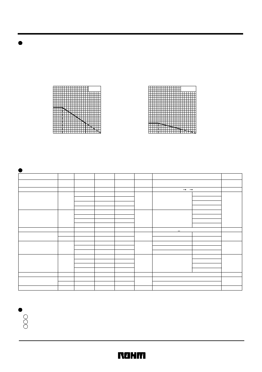
When it is used in the ambient temperature of (Ta)=25∞C and more, make reference to each thermal derating
characteristics of used package. Both Fig.5 and Fig.6 show these characteristic when ROHM's standard board
(70mmX70mmX1.6mm, glass epoxy board) is mounted.
Power consumption of the IC
SSOP5
(SMP5C2) package
VSOF5
(EMP5) package
Fig.5 Thermal derating curve
Fig.6 Thermal derating curve
Circuit current at ON/OFF is very small. Power consumption in output depends on each load connected with
V
OUT
pin. Please note that total power consumption must be within a power dissipation range in the secure area
of the entire operating temperature. Power dissipation of these packages; SSOP5
(SMP5C2)
package (BD52XXG/
BD53XXG) Fig.5, and VSOF5
(EMP5)
package (BD52XXFVE/BD53XXFVE) Fig.6 is shown below.
Electrical characteristics (
Unless otherwise noted; Ta=-25∞C ~ 85∞C)
1 Detection voltage (V
DET
) : V
DD
voltage when the output (Vout) goes from "H" to "L" .
2 Release voltage (V
DET
+V
DET
) : V
DD
voltage when output (Vout) goes from "L" to "H" .
3 Hysteresis voltage (V
DET
) : The difference between detection voltage and release voltage. Malfunction
due to noise in V
DD
(within hysteresis voltage) could be avoided by hysteresis
voltage.
Term explanation
4/15
Voltage detectors
BD52XXG/FVE
BD53XXG/FVE
P
o
w
e
r
d
i
s
s
i
p
a
t
i
o
n
(
m
W
)
P
o
w
e
r
d
i
s
s
i
p
a
t
i
o
n
(
m
W
)
Ambient temperature Ta(∞C)
Ambient temperature Ta(∞C)
75
100
125
600
800
25
50
200
210
400
0
BD52XXFVE
BD53XXFVE
75
100
125
600
540
800
25
50
200
400
0
BD52XXG
BD53XXG
Circuit current
when ON
Circuit current
when OFF
Output leak current
Hysteresis voltage
Detection voltage
temperature coefficient
*1 Operation is guaranteed for Ta=25∞C.
Note) R
L
is not necessary for CMOS output type.
Note) Minimum operating voltage
V
OUT
output becomes inconsistent if the V
DD
is equal to or lower than the operating limit voltage. It goes open, H, or L.
Note) Hysteresis voltage=(Reset release voltage)-(Reset detection voltage) [V]
Min. operating voltage
"H" output current
(Only BD53XXG/FVE series)
CT pin
Threshold voltage
"L" output current
--
--
--
--
--
0.90
0.80
0.85
0.90
--
2.70
--
0.80
2.40
V
DET
=2.3~3.1V
--
0.85
2.55
V
DET
=3.2~4.2V
V
DET
=4.3~5.2V
--
0.95
2.85
V
DET
=5.3~6.0V
V
DET
=3.2~4.2V
V
DET
=4.3~5.2V
V
DET
=5.3~6.0V
--
0.75
V
DET
=2.3~3.1V
2.25
2.40
2.55
2.70
0.1
µ
A
µ
A
µ
A
I
DD1
I
DD2
I
leak
V
DET
X0.03 V
DET
X0.05 V
DET
X0.08
V
V
DET
RL=470k, V
DD
=L H L
V
DET
/T
--
±
100
±
360
ppm/∞C
V
DD
=V
DET
≠0.2V
V
DD
=V
DET
+2.0V
0.95
--
--
V
V
OPL
R
L
=470k, V
OL
0.4V
V
DD
=V
DS
=10V
*1
0.7
1.4
--
0.9
1.8
--
1.1
2.2
--
mA
I
OH
V
CTH
R
CT
V
DS
=0.5V, V
DD
=4.8V
V
DET
=2.3~6.0V
V
DS
=0.5V, V
DD
=6.0V
V
DET
=2.7~6.0V
V
DET
=2.3~4.2V
V
DET
=4.3~5.2V
V
DS
=0.5V, V
DD
=8.0V
V
DET
=5.3~6.0V
2.0
5.0
--
mA
I
OL1
I
OL2
0.4
1.2
--
V
DS
=0.5V, V
DD
=1.2V
V
DS
=0.5V, V
DD
=2.4V
V
DD
X0.5
V
DD
X0.4
V
DET
=2.3~2.6V
V
DD
X0.45
V
DET
=2.7~4.2V
V
DET
=4.3~5.2V
V
DD
X0.5
V
DD
X0.6
V
DD
X0.6
V
DD
X0.6
V
DD
X0.6
V
DD
X0.35
V
DD
X0.3
V
DD
X0.3
V
DD
X0.4
V
DET
=5.3~6.0V
V
V
DD
=V
DET
X1.1
R
L
=470k
Symbol
Min.
Max.
Unit
Conditions
Fig.24
Fig.27
Fig.29
Fig.33
5.5
9
12.5
M
CT pin
V
DD
=V
DET
X1.1, V
CT
=0.5V
*1
Fig.31
Fig.26
Fig.34
Fig.35
Fig.36
Fig.25
150
240
--
µ
A
I
CT1
I
CT2
CT pin "L" current
15
40
--
V
CT
=0.1V,V
DD
=0.95V
*1
V
CT
=0.5V,V
DD
=1.5V
Reference
Data
Typ.
Parameter
Operating explanation
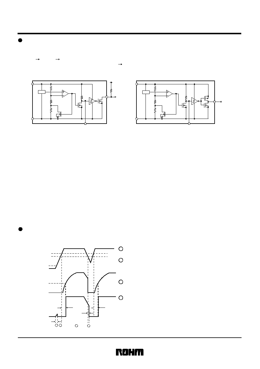
∑When V
DD
is equal to or more than the release voltage (V
DET
+V
DET
), CT pin voltage becomes V
DD
(External capacitor is in charging mode.) and output V
OUT
is in "H" mode. (Nch output transistor Q1 is OFF,
Pch output transistor Q2 is ON.) When V
DD
is gradually decreased, Q3 connected to CT pin in the detection
voltage (V
DET
) switches OFF to ON, external capacitor is discharged, and CT pin voltage becomes
decreased. When the CT pin voltage is lower than the threshold voltage of next inverter, output (V
OUT
) turns
"L". (Nch output transistor Q1 is ON, Pch output transistor Q2 is OFF.)
∑ When V
DD
is equal to or lower than the detection voltage (V
DET
), CT pin voltage is L voltage (External
capacitor is in discharging mode and Q3 is ON), output V
OUT
is in "L" mode. When V
DD
is gradually
increased, Q3 is OFF in the release voltage (V
DET
+V
DET
) and CT pin external capacitor becomes to be
charged through resistor R1 in the IC. When the CT pin voltage is more than the threshold voltage of next
inverter, output (V
OUT
) goes from "L" to "H". (Nch output transistor Q1 is OFF, Pch output transistor Q2 is
ON.) Delay time is the time when output V
OUT
goes from "L" to "H" after the V
DD
is more than the release
voltage. (V
DET
+V
DET
) Delay time can be set freely by the CT pin external capacitor. (Usage is shown at P10)
Ex.) For both open drain type (Fig.7) and CMOS output type (Fig.8), detection voltage and release voltage are
threshold voltage. When voltage applied to V
DD
pin reaches each threshold voltage, V
OUT
pin voltage goes
"H" "L" or "L" "H'. BD52XXG/FVE and BD53XXG/FVE incorporate delay time circuit that can set delay time
by the external capacitor when output goes"L" "H". BD52XXG/FVE series are open drain types and pull-up
resistor must be connected to V
DD
, or other power supply. (In this case, output (V
OUT
) H voltage is V
DD
, or
other power supply voltage.)
Ex.) The relation between input voltage V
DD
and output voltage V
OUT
when V
DD
is increased and decreased
is shown below. (Circuit is shown in Fig7, Fig.8)
∑ SWEEP DOWN for V
DD
∑ SWEEP UP for V
DD
∑Some hysteresis is given such a way that the release voltage is the detection voltageX(1.05 Typ.).
∑ The output becomes inconsistent if the V
DD
is equal to or lower than the operating limit voltage.
R1
R2
R3
Q3
Q1
V
ref
Vout
V
DD
V
DD
Reset
CT
GND
GND
Fig.7 (BD52XX type Internal block diagram)
Fig.8 (BD53XX Internal block diagram)
Timing waveform
If the V
DD
is equal to or lower than the operating limit
voltage (V
OPL
) at power-up, the output is inconsistent.
If the V
DD
goes below the detection voltage (V
DET
) at
power-down or instantaneous power failure, V
OUT
turns L
with a delay of T
PHL
. See Fig.16 for the reference waveform.
The potential difference between the detection voltage and
the release voltage is called hysteresis (V
DET
).
The products are designed so as to prevent power supply
fluctuation within this hysteresis from causing fluctuation in
output in order to avoid malfunction due to noise.
When the V
DD
is equal to or more than reset release voltage
(V
DET
+V
DET
), V
OUT
goes from "L" to "H" with a delay
of T
PLH
set by the capacitor that is connected to CT pin.
When the V
DD
is equal to or more than the V
OPL
and the
V
DD
is equal to or more than the reset release voltage
(V
DET
+V
DET
), CT pin voltage (V
CT
) is "L" and output
(V
OUT
) is also "L".
Fig.9
R1
R2
R3
Q1
Q3
Q2
V
DD
Vref
Reset
Vout
CT
V
DD
GND
2
1
3
4
See Fig.16 and 18 for the reference waveform.
The potential difference between the detection voltage
and the release voltage is called hysteresis (Vs).
The products are designed so as to prevent power supply
fluctuation within this hysteresis from causing fluctuation
in output in order to avoid malfunction due to noise.
5/15
Voltage detectors
BD52XXG/FVE
BD53XXG/FVE
2
1
3
4
V
DD
V
DD
1/2 V
DD
V
DD
V
OUT
V
CT
V
IN
V
DET
0V
V
OPL
V
DET
+V
DET
T
PHL
T
PLH
T
PLH