 | ÐлекÑÑоннÑй компоненÑ: BD6155FVM | СкаÑаÑÑ:  PDF PDF  ZIP ZIP |
Äîêóìåíòàöèÿ è îïèñàíèÿ www.docs.chipfind.ru
BD6155FVM
Communication ICs
1/7
DC/DC converter for LCD back light
BD6155FVM
BD6155FVM is an ideal IC to drive white LED used for the LCD back light of cellular phones, and PDA etc.
This IC incorporates charging pump step-up circuit to drive white LED with high V
F
. It also integrates a driver to drive
white LED with 4-step constant current. Only one external resistor can set the current value.
!
Applications
Small portable appliances, such as cellular phones, PHS, PDA
Battery-powered equipments using the white LED.
!
Features
1) Built-in charging pump step-up circuit.
2) Built-in constant current driver for LED. (Current value : 4 steps variable)
3) Ultra small MSOP8 package. (Height 0.9mm Max.)
!
!
!
!
Absolute maximum ratings (Ta=25
°C)
Parameter
Symbol
Limits
Unit
Pd
350
mW
Power dissipation
Maximum supply voltage
V
BAT
V
-
0.3~
+
6.0
Maximum input voltage
-
0.3~
+
6.0
V
IN
V
Topr
°
C
Operating temperature
-
25~
+
75
Storage temperature
Tstg
-
55~
+
125
°
C
Reduce to 3.5mW/
°
C when Ta=25
°
C or above.
!
!
!
!
Recommended operating conditions (Ta=25
°C)
Parameter
Power supply
V
BAT
2.9
5.5
V
-
Symbol
Min.
Typ.
Max.
Unit
BD6155FVM
Communication ICs
2/7
!
!
!
!
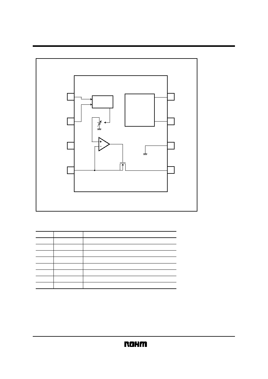
Block diagram
CHARGE
PUMP
DRIVER
CURRENT
CONT
1
2
3
4
CURRENT1
CURRENT2
STBY
LEDS
8
V
BAT
C
GND
LED
7
6
5
!
!
!
!
Pin descriptions
Pin No.
3
Stand-by pin (High:Operation, Low:No operation)
4
LED driver current pin (Fixed current sink pin)
2
Fixed current setup pin2.
1
Pin Name
STBY
LEDS
5
LED cathode connection pin for charge pump
LED
CURRENT2
7
Capacitor connection pin for charge pump
6
Ground
C
8
Power supply voltage input pin
VBAT
GND
CURRENT1
Fixed current setup pin1.
Function
BD6155FVM
Communication ICs
3/7
!
!
!
!
Electrical characteristics (unless otherwise noted, Ta=25
°C, VBAT=3.6V, STBY=3.6V)
Parameter
Symbol
Min.
I
Q
1
I
Q
2
fosc
VDC1
VDC2
-
-
-
-
4.4
4.8
250
Typ.
0.3
120
5.6
4.8
Max.
Unit
1.0
mA
5
µ
A
-
-
V
kHz
-
V
700
k
Conditions
<LED+Charge pump block>
Circuit current
Standby current
<Fixed current driver for LED>
<Charge pump>
Output voltage 1
Oscillator frequency
Active
Stand-by
Hi
Low
Output voltage 2
Stand-by pin pull down resistor
This product is not designed for protection against radioactive rays.
No load
No load, STBY
=
0V
ILEDMAX
-
-
80
mA
LED max drive current
Ron7
-
3
7
V
NMOS ON resistance
Drive current 80mA
VLED1
184
205
226
mV
Current control setup voltage 1
CURRENT2=High, CURRENT1=High
VLED2
131
155
179
mV
Current control setup voltage 2
CURRENT2=High, CURRENT1=LOW
VLED3
89
105
121
mV
Current control setup voltage 3
CURRENT2=LOW, CURRENT1=High
VLED4
42
55
68
mV
Current control setup voltage 4
CURRENT2=LOW, CURRENT1=LOW
V
IH
V
IL
2.0
-
-
-
V
Fixed current setup pin
control voltage
VBAT=3.6V, I
O
=80mA charge pump output monitor RB521-S30 use
VBAT=3.2V, I
O
=60mA charge pump output monitor RB521-S30 use
V
IH
V
IL
-
0.3
-
0.3
-
-
0.3
0.3
V
RSTBY
2.0
400
-
V
Stand-by pin control
voltage
!
!
!
!
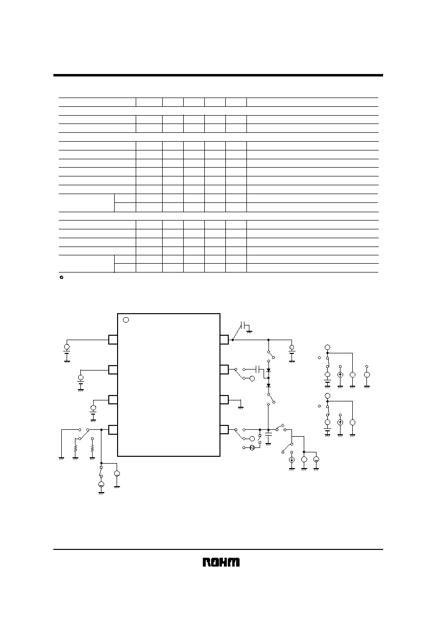
Measurement circuit
1
CURRENT1
VBAT
C+
GND
LED
CURRENT2
STBY
LEDS
2
3
4
8
7
6
5
SWD1
AM8
V8
OPEN
OPEN
OPEN
OPEN
OPEN
ON
ON
ON
ON
ON
AM4
SW4B
VM4
VO1
VA01
C1
SW7
SW5
SW4
R=2.7
R=20K
C2
SWD2
SWO3
SWO1
SWO2
ISO1
D1
D2
1
2
1
1
2
2
3
3
2
1
1
µ
F
Fig.1
A
7
5
5
V1
AM1
A
V2
AM2
A
V3
AM3
A
V
V
V
V
SW52
AM52
IS52
VM52
V52
V
A
OPEN
1
2
3
7
SW72
AM72
IS72
VM72
V72
V
A
FM72
F
BD6155FVM
Communication ICs
4/7
!
!
!
!
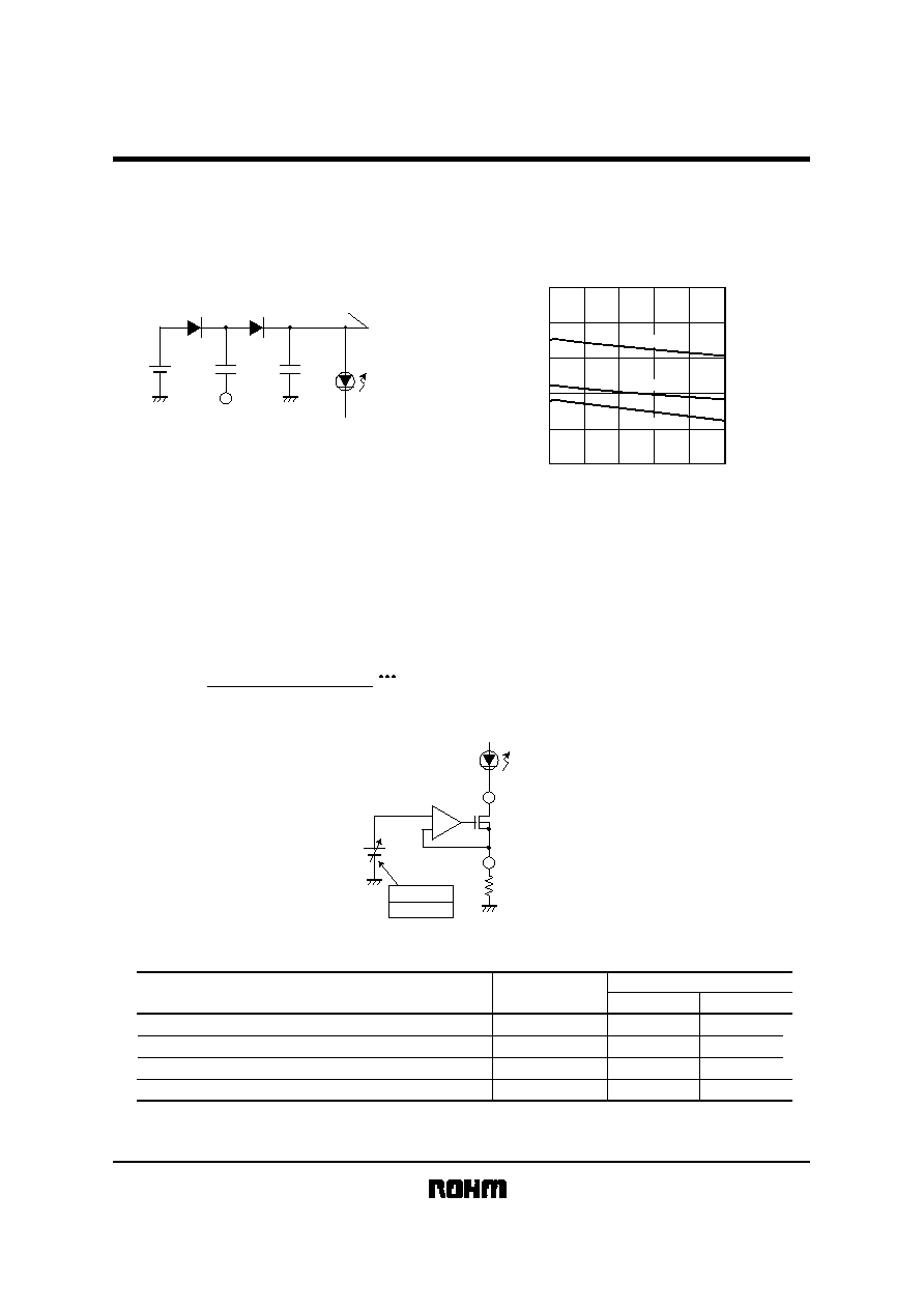
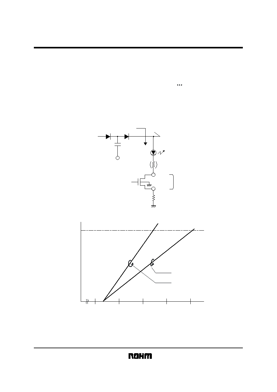
Circuit operation
1) Charge pump driver
Charge pump is consisted capacitor pin (pin7), external schotky diodes and capacitors.
Output voltage at no loading is 2VBAT-2VF. (VF is as same as schotky's VF )
Output voltage at loading is referred Fig2. As standard example, however it depends on external components.
VBAT
Shotky diodes
RB521-S30
Charge pump output
LED
1
µ
F
C (Pin7)
1
µ
F
20
40
0
60
80
100
15
3
0
6
9
12
OUTPUT VOLTAGE : (V)
OUTPUT LOAD : (mA)
Fig.2 Charge pump loading characteristics
(Typical operating characteristics)
VBAT=2.9V
VBAT=3.6V
VBAT=5.5V
2) Fixed current driver
LED driver fixed current is determined by resistor value between LEDS pin (pin4) and GND.
At current control set up voltage1 (Current1, 2=High) resistor value between LEDS-GND is set as 2.7
.
205mV
÷
2.7
= 75.9mA (2 expressions)
The above current is loaded to LED as fixied current.
LED
LED (5Pin)
+
-
LEDS (4Pin)
RSENSE
CURRENT1
CURRENT2
· LED drive current fix example
LEDS pin voltage
(mV)
LED drive current (mA)
RSENSE=2.7
RSENSE=5.1
105.0
38.9
20.6
Current control setup voltage 1 (Current 1=High Current 2=High)
Current control setup voltage 2 (Current 1=Low Current 2=High)
Current control setup voltage 3 (Current 1=High Current 2=Low)
Current control setup voltage 4 (Current 1=Low Current 2=Low)
205.0
40.2
75.9
57.4
155.0
30.4
55.0
10.8
20.4
The less RSENSE, the bigger fixed current for LED drive.
Resistors value should be determined with confirmation of charge pump loading characteristics (Fig.2) and LED's I-V characteristics.
BD6155FVM
Communication ICs
5/7
!
!
!
!
Design information
1. The maximum of power loss of this IC is controlled by the output transistor M1 in regulator driver.
Relations of the power supply voltage are signified in 2 expressions with this loss.
V = V
OUT
-
(VF2
+
ILED
×
R1
+
VLED)
The loss in M1,
V
×
ILED = ILED
×
{2VBAT
-
(2VF1
+
VF2
+
ILED
×
R1
+
VLED)} (2 expressions)
V ; The voltage between LED-LEDS
VF1 ; Shotky's Di VF
VF2 ; LED's VF
V
OUT
; Charge pump output voltage (Fig.2)
VLED ; The voltage across RSENSE (examples at 205mV calculation)
ILED ; Drive current.
V
BAT
0.2V
M1
V
OUT
V
VF1
ILED
VF1
VF2
LED
LED
R1
LEDS
RSENS
2
0
100
200
300
Room temperature power dissipation
(350mW)
Power supply voltage V
BAT
(V)
VF1=0.5V
VF2=3.4V
R1=0
Loss Pd : (mW)
Pd-V
BAT
I
O
=50mA
I
O
=80mA
3
4
5
6
2) Power supply voltage
The thermal shutdown circuit turn on, and output electric current declines when chip temperature is about 125 degrees
due to low electric current driver.
Document Outline