 | –≠–ª–µ–∫—Ç—Ä–æ–Ω–Ω—ã–π –∫–æ–º–ø–æ–Ω–µ–Ω—Ç: BR24E16 | –°–∫–∞—á–∞—Ç—å:  PDF PDF  ZIP ZIP |
BR24C08 / BR24C08F / BR24C08FJ / BR24C08FV / BR24C16/ BR24C16F /
Memory Ics
BR24C16FJ /
BR24C16FV / BR24E16 / BR24E16F / BR24E16FJ / BR24E16FV
I
2
C BUS compatible serial EEPROM
BR24C08 / BR24C08F / BR24C08FJ / BR24C08FV /
BR24C16 / BR24C16F / BR24C16FJ / BR24C16FV /
BR24E16 / BR24E16F / BR24E16FJ / BR24E16FV /
The BR24C08, BR24C16 and BR24E16 series are 2-wire (I
2
C BUS type) serial EEPROMs which are electrically
programmable.
I
2
C BUS is a registered trademark of Philips.
Features
1) 1k x 8 bits serial EEPROM.
(BR24C08 / F / FJ / FV)
2k x 8 bits serial EEPROM.
(BR24C16 / F / FJ / FV, BR24E16 / F / FJ / FV)
2) Two wire serial interface.
(2Byte Address : BR24E16)
3) Operating voltage range : 2.7V
5.5V
4) Low current consumption
Active (at 5V) : 2.0mA (Typ.)
Standby (at 5V) : 1.0
µ
A (Typ.)
5) Auto erase and auto complete functions can be used
during write operations.
6) Page write function : 16byte
7) DATA security
Write protect feature
Inhibit to WRITE at low Vcc
8) Noise filters at SCL and SDA pins.
9) Address can be incremented automatically during
read operations.
10) Compact packages.
11) Rewriting possible up to 100,000 times.
12) Data can be stored for ten years without corruption.
Absolute maximum ratings (Ta=25
∞
C)
Parameter
Symbol
Limits
Unit
Supply voltage
-
0.3
~
+
6.5
V
Power dissipation
mW
Storage temperature range
-
65
~
+
125
∞
C
Operating temperature range
∞
C
Terminal voltage
-
V
-
40
~
+
85
V
CC
-
0.3
~V
CC
+
0.3
Pd
Tstg
Topr
300(SSOP
-
B8)
1
800(DIP8)
450(SOP8, SOP
-
J8)
2
3
1 Reduced by 3.0mW for each increase in Ta of 1
∞
C over 25
∞
C.
2 Reduced by 3.5mW for each increase in Ta of 1
∞
C over 25
∞
C.
3 Reduced by 5.0mW for each increase in Ta of 1
∞
C over 25
∞
C.
Recommended operating conditions (Ta=25
∞
C)
Parameter
Symbol
Limits
Unit
Power supply voltage
V
Input voltage
V
IN
V
V
CC
0
~V
CC
2.7
~5.5
BR24C08 / BR24C08F / BR24C08FJ / BR24C08FV / BR24C16/ BR24C16F /
Memory Ics
BR24C16FJ /
BR24C16FV / BR24E16 / BR24E16F / BR24E16FJ / BR24E16FV
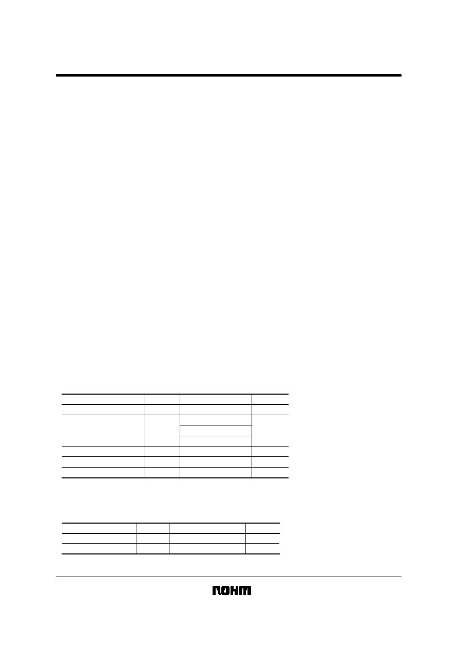
Block diagram
BR24C08 / F / FJ / FV
8kbits EEPROM ARRAY
CONTROL LOGIC
HIGH VOLTAGE GEN.
ACK
START
STOP
10bits
10bits
8bits
DATA
REGISTER
ADDRESS
DECODER
A0
A1
A2
1
2
3
4
GND
WP
SCL
SDA
8
7
6
5
V
CC
V
CC
LEVEL DETECT
ADDRESS REGISTER
SLAVE WORD
∑
Function
Slave address set
Serial clock input
serial data input, serial data output
Wite protect pin
Power supply
Pin name
A0, A1
A2
SCL
SDA
WP
V
CC
GND
I / O
I / O
-
-
-
I
I
I
Ground (0V)
Out of use. Please connect to GND.
Slave and word address,
An open drain output requires a pull-up resistor.
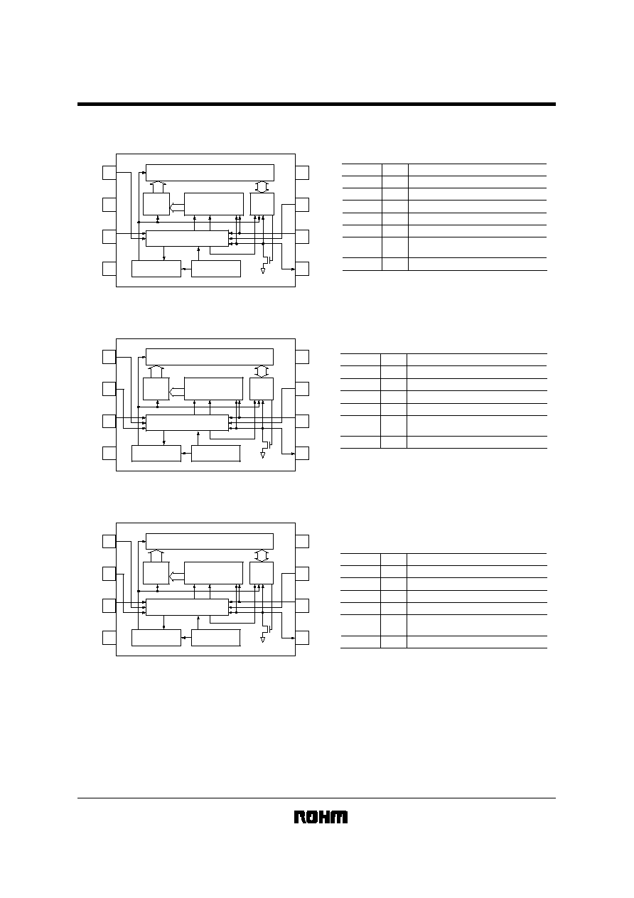
BR24C16 / F / FJ / FV
16kbits EEPROM ARRAY
CONTROL LOGIC
HIGH VOLTAGE GEN.
ACK
START
STOP
11bits
8bits
DATA
REGISTER
ADDRESS
DECODER
A0
A1
A2
1
2
3
4
GND
WP
SCL
SDA
8
7
6
5
V
CC
V
CC
LEVEL DETECT
ADDRESS REGISTER
SLAVE WORD
∑
11bits
A0, A1, A2
SCL
SDA
WP
V
CC
GND
I / O
I / O
-
-
I
I
I
Function
Pin name
An open drain output requires a pull-up resistor.
Serial clock input
serial data input, serial data output
Wite protect pin
Power supply
Ground (0V)
Out of use. Please connect to GND.
Slave and word address,
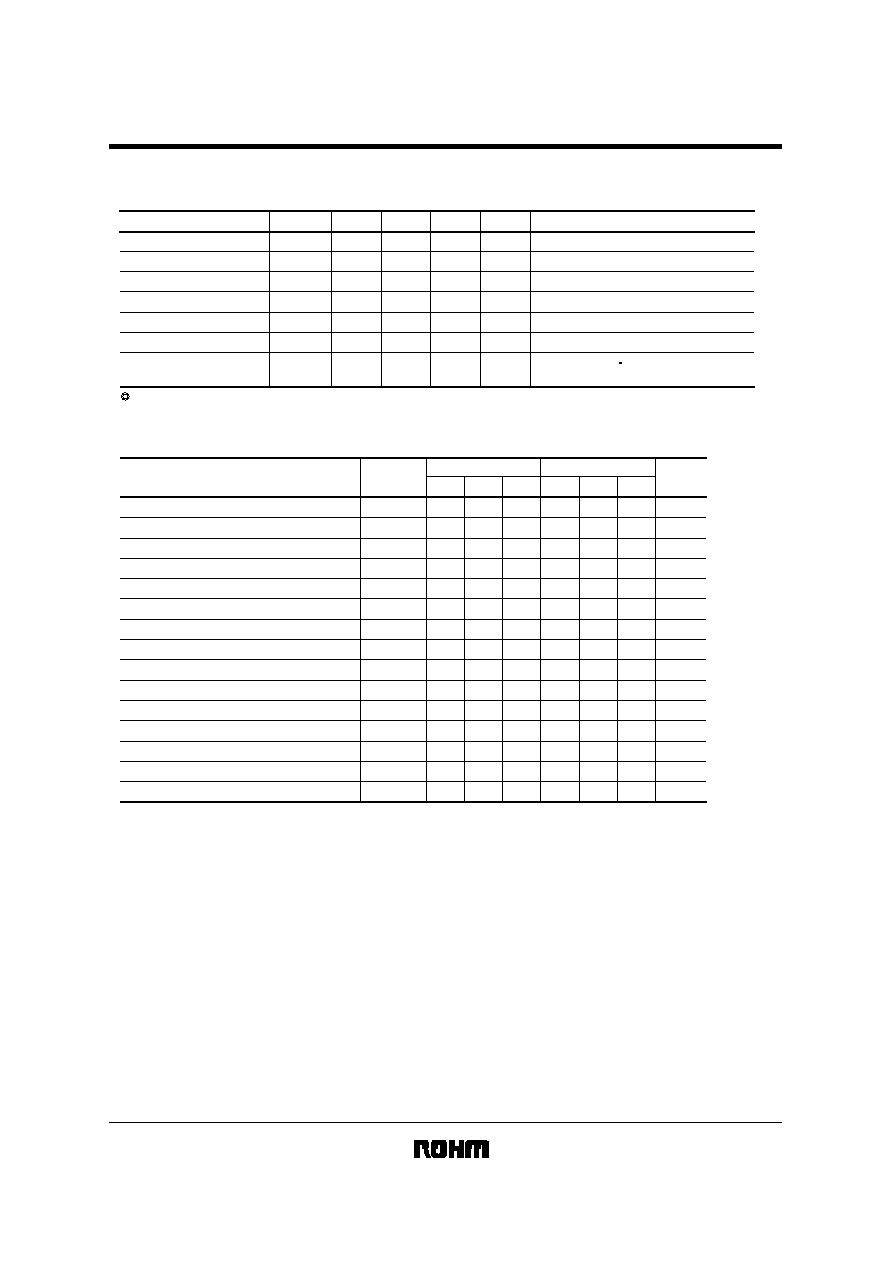
BR24E16 / F / FJ / FV
16kbits EEPROM ARRAY
CONTROL LOGIC
HIGH VOLTAGE GEN.
ACK
START
STOP
11bits
8bits
DATA
REGISTER
ADDRESS
DECODER
A0
A1
A2
1
2
3
4
GND
WP
SCL
SDA
8
7
6
5
V
CC
V
CC
LEVEL DETECT
ADDRESS REGISTER
SLAVE WORD
∑
11bits
A0, A1, A2
SCL
SDA
WP
V
CC
GND
I / O
I / O
-
-
I
I
I
Function
Pin name
An open drain output requires a pull-up resistor.
Serial clock input
serial data input, serial data output
Wite protect pin
Power supply
Ground (0V)
Slave and word address,
Slave address set
BR24C08 / BR24C08F / BR24C08FJ / BR24C08FV / BR24C16/ BR24C16F /
Memory Ics
BR24C16FJ /
BR24C16FV / BR24E16 / BR24E16F / BR24E16FJ / BR24E16FV
Electrical characteristics
DC characteristics (Unless otherwise noted, Ta=
-
40
85
∞
C, V
CC
=2.7
5.5V)
Parameter
Symbol
Min.
Typ.
Max.
Unit
Conditions
V
IH
-
-
V
V
IL
-
-
0.3V
CC
V
V
OL
-
-
0.4
V
Input leakage current
I
LI
-
1
µ
A
V
IN
=
0V
~V
CC
Output leakage current
I
LO
-
1
-
1
-
1
µ
A
operating current
I
CC
-
3.0
mA
Standby current
I
SB
-
-
-
3.0
µ
A
0.7V
CC
-
-
I
OL
=
3.0mA(SDA)
V
CC
=
5.5V, f
SCL
=
400kHz
A0, A1, A2
=
GND, WP
=
GND
V
OUT
=
0V
~V
CC
"HIGH" input voltage
"LOW" input voltage
"LOW" output voltage
V
CC
=
5.5V, SDA SCL
=
V
CC
This product is not designed for protection against radioactive rays.
Operating timing characteristics (Unless otherwise noted, Ta=
-
40
85
∞
C, V
CC
=2.7
5.5V)
Parameter
Symbol
Vcc
=
5V
±
10%
Vcc
=
3V
±
10%
Unit
f
SCL
kHz
t
HIGH
Noise erase valid time (SDA/SCL pins)
t
I
µ
s
Dataclock "HIGH" time
SCL frequency
µ
s
Dataclock "LOW" time
t
LOW
µ
s
SDA / SCL rise time
t
R
µ
s
SDA / SCL fall time
t
F
µ
s
Start condition hold time
t
HD
: STA
µ
s
Start condition setup time
t
SU
: STA
µ
s
Input data hold time
t
HD
: DAT
ns
Input data setup time
t
SU
: DAT
ns
Output data delay time
t
PD
µ
s
Output data hold time
t
DH
µ
s
Stop condition setup time
t
SU
: STO
µ
s
Bus open time before start or transfer
t
BUF
µ
s
t
WR
Min.
-
0.6
-
1.2
-
-
0.6
0.6
0
100
0.1
0.1
0.6
1.2
-
Typ.
-
-
-
-
-
-
-
-
-
-
-
-
-
-
-
Max.
400
-
0.05
-
0.3
0.3
-
-
-
-
0.9
-
-
-
10
Min.
-
4.0
-
4.7
-
-
4.0
4.7
0
250
0.2
0.2
4.7
4.7
-
Typ.
-
-
-
-
-
-
-
-
-
-
-
-
-
-
-
Max.
100
-
0.1
-
1.0
0.3
-
-
-
-
3.5
-
-
-
10
ms
Internal write cycle time

BR24C08 / BR24C08F / BR24C08FJ / BR24C08FV / BR24C16/ BR24C16F /
Memory Ics
BR24C16FJ /
BR24C16FV / BR24E16 / BR24E16F / BR24E16FJ / BR24E16FV
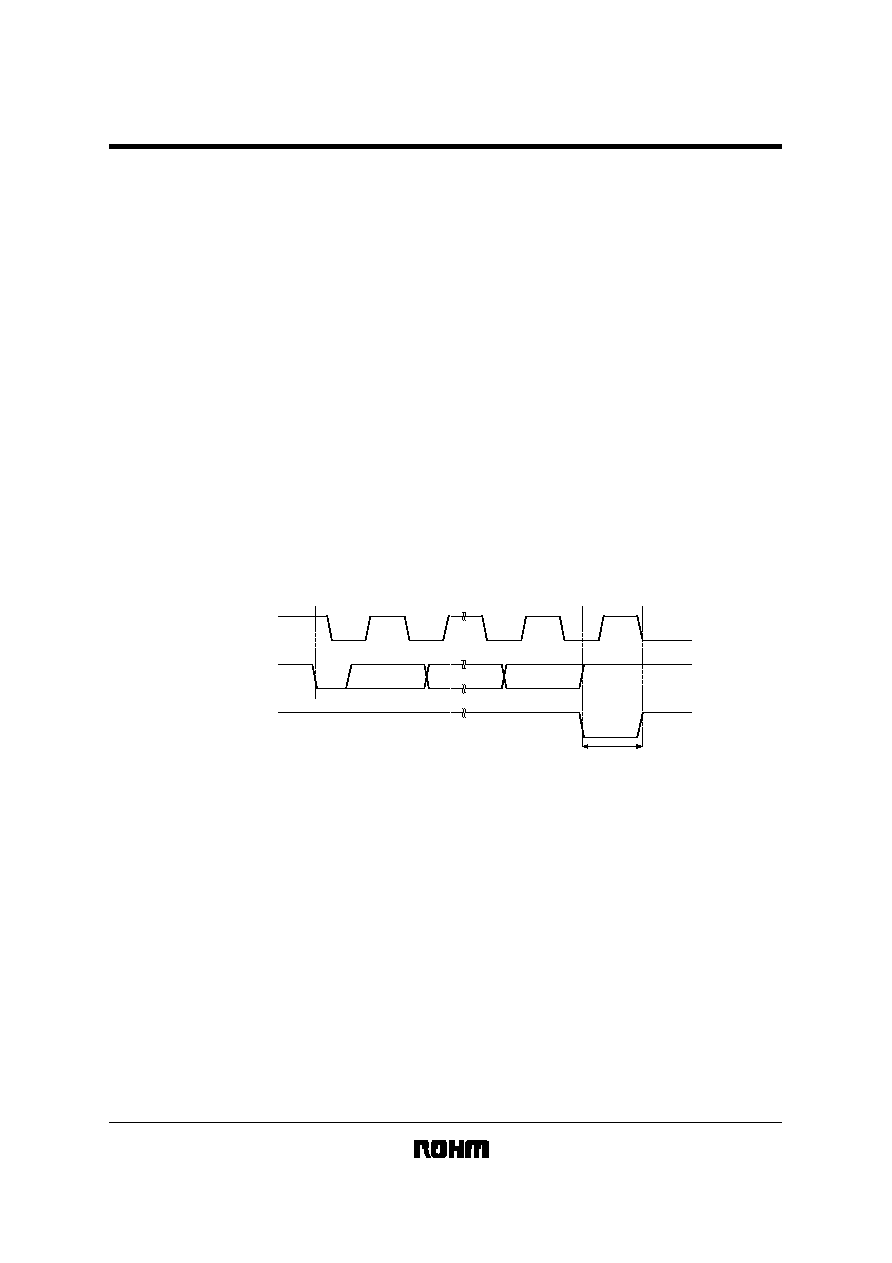
Timing charts
t
BUF
t
DH
t
PD
t
HIGH
t
HD
:
STA
t
LOW
t
F
t
R
SDA
SDA
SCL
START BIT
STOP BIT
SCL
SDA
Data is read on the rising edge of SCL.
Data is output in synchronization with the falling edge of SCL.
t
SU
:
DAT
t
HD
:
DAT
t
SU
:
STO
t
HD
:
STA
t
SU
:
STA
(OUT)
(IN)
Fig.1 Synchronized data input / output timing
ACK
D0
t
WR
SDA
SCL
START CONDITION
STOP CONDITION
Write data (n)
Fig.2 Write cycle timing
Circuit operation
(1) Start condition (recognition of start bit)
Before executing any command, when SCL is HIGH, a start condition (start bit) is required to cause SDA to fall from
HIGH to LOW. This IC is designed to constantly detect whether there is a start condition (start bit) for the SDA and
SCL line, and no commands will be executed unless this condition is satisfied.
(See Fig.1 for the synchronized data input / output timing.)
(2) Stop condition (recognition of stop bit)
To stop any command, a stop condition (stop bit) is required. A stop condition is achieved when SDA goes from LOW
to HIGH while SCL is HIGH. This enables commands to be completed.
(See Fig.1 for the synchronized data input / output timing.)
(3) Precautions concerning write commands
In the WRITE mode, the transferred data is not written to the memory unless the stop bit is executed.
BR24C08 / BR24C08F / BR24C08FJ / BR24C08FV / BR24C16/ BR24C16F /
Memory Ics
BR24C16FJ /
BR24C16FV / BR24E16 / BR24E16F / BR24E16FJ / BR24E16FV
(4) Device addressing
BR24C08 / F / FJ / FV
1) Make sure the slave address is output from the master in continuation with the start condition.
2) The upper 4bits of the slave address are used to determine the device type. The device code for this IC is fixed at
"1010".
3) The next 1bit of the slave address (A2 ... device address) are used to select the device. This IC can address up to
two devices on the same bus.
4) The next 2bits (P1, P0 ... page select) are used by the master to select four 256 word page of memory.
P1, P0 set to `0' `0'
$ $ $ $ $ $ $
1 page (000 ~0FF)
P1, P0 set to `0' `1'
$ $ $ $ $ $ $
2 page (100 ~1FF)
P1, P0 set to `1' `0'
$ $ $ $ $ $ $
3 page (200 ~2FF)
P1, P0 set to `1' `1'
$ $ $ $ $ $ $
4 page (300 ~3FF)
5) The lowermost bit of the slave address (R / W ... READ / WRITE) is used to set the write or read mode as follows.
R / W set to 0 ... Write
(Random read word address setting is also 0)
R / W set to 1 ... Read
A2
P1
P0
1010
R / W
BR24C16 / F / FJ / FV
1) Make sure the slave address is output from the master in continuation with the start condition.
2) The upper 4bits of the slave address are used to determine the device type. The device code for this IC is fixed at
"1010".
3) The next 3bits (P2, P1, P0 ... page select) are used by the master to select four 256 word page of memory.
P2, P1, P0 set to `0' `0' `0'
$ $ $ $ $ $ $
1 page (000 ~0FF)
P2, P1, P0 set to `0' `0' `1'
$ $ $ $ $ $ $
2 page (100 ~1FF)
:
:
P2, P1, P0 set to `1' `1' `1'
$ $ $ $ $ $ $
8 page (700 ~7FF)
4) The lowermost bit of the slave address (R / W ... READ / WRITE) is used to set the write or read mode as follows.
R / W set to 0 ... Write
(Random read word address setting is also 0)
R / W set to 1 ... Read
P2
P1
P0
1010
R / W
BR24E16 / F / FJ / FV
1) Make sure the slave address is output from the master in continuation with the start condition.
2) The upper 4bits of the slave address are used to determine the device type. The device code for this IC is fixed at
"1010".
3) The next 3bits of the slave address (A2, A1, A0 ... device address) are used to select the device. This IC can
address up to eight devices on the same bus.
4) The lowermost bit of the slave address (R / W ... READ / WRITE) is used to set the write or read mode as follows.
R / W set to 0 ... Write
(Random read word address setting is also 0)
R / W set to 1 ... Read
A2
A1
A0
1010
R / W
BR24C08 / BR24C08F / BR24C08FJ / BR24C08FV / BR24C16/ BR24C16F /
Memory Ics
BR24C16FJ /
BR24C16FV / BR24E16 / BR24E16F / BR24E16FJ / BR24E16FV
(5) Write protect (WP)
When WP pin set to V
CC
(High level), write protect is set by all address. When WP pin set to GND (Low level), enable
to write to all address. Either control this pin or connect to GND (or V
CC
). It is inhibited from being left unconnected.
(6) ACK signal
The acknowledge signal (ACK signal) is determined by software and is used to indicate whether or not a data transfer
is proceeding normally. The transmitting device, whether the master or slave, opens the bus after an 8-bit data output
(
µ
-COM when a write or read command of the slave address input ; this IC when reading data).
For the receiving device during the ninth clock cycle, SDA is set to LOW and an acknowledge signal (ACK signal) is
sent to indicate that it received the 8-bit data (this IC when a write command or a read command of the slave address
input,
µ
-COM when a read command data output).
The ICs output a LOW acknowledge signal (ACK signal) after recognizing the start condition and slave address (8
bits).
When data is being write to the ICs, a LOW acknowledge signal (ACK signal) is output after the receipt of each 8 bits
of data (word address and write data).
When data is being read from the IC, 8bits of data (read data) are output and the IC waits for a returned LOW
acknowledge signal (ACK signal). When an acknowledge signal (ACK signal) is detected and a stop condition is not
sent from the master (
µ
-COM) side, the IC continues to output data. If an acknowledge signal (ACK signal) is not
detected, the IC interrupts the data transfer and ceases reading operations after recognizing the stop condition (stop
bit). The IC then enters the waiting or standby state.
(See Fig.3 for acknowledge signal (ACK signal) response.)
1
8
9
SCL
SDA
SDA
Start condition
(start bit)
Acknowledge signal
(ACK signal)
(from
µ
-COM)
output data)
(
µ-
COM
(IC output data)
Fig.3 Acknowledge (ACK signal) response
(during write and read slave address input)
BR24C08 / BR24C08F / BR24C08FJ / BR24C08FV / BR24C16/ BR24C16F /
Memory Ics
BR24C16FJ /
BR24C16FV / BR24E16 / BR24E16F / BR24E16FJ / BR24E16FV
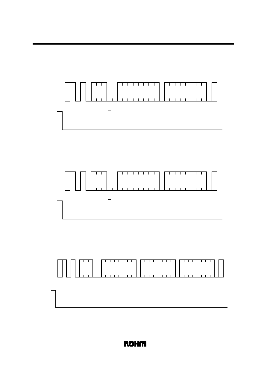
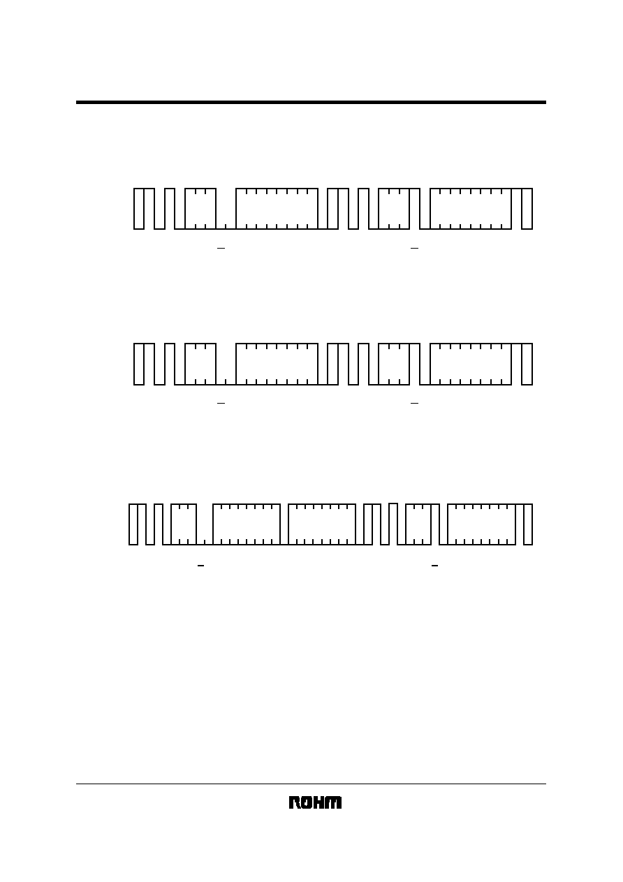
(7) Byte write
BR24C08 / F / FJ / FV
1
0
1
0 A2 P1 P0
D7
D0
S
T
O
P
DATA
A
C
K
A
C
K
A
C
K
WORD
ADDRESS
R
/
W
W
R
I
T
E
SLAVE
ADDRESS
S
T
A
R
T
SDA
LINE
WP
Fig.4
WA
7
WA
0
BR24C16 / F / FJ / FV
1
0
1
0 P2 P1 P0
D7
D0
S
T
O
P
DATA
A
C
K
A
C
K
A
C
K
WORD
ADDRESS
R
/
W
W
R
I
T
E
SLAVE
ADDRESS
S
T
A
R
T
SDA
LINE
WP
Fig.5
WA
7
WA
0
BR24E16 / F / FJ / FV
SDA
LINE
WP
S
T
A
R
T
SLAVE
ADDRESS
1 0
0
1
A2 A1 A0
R
/
W
W
R
I
T
E
D7
DATA
D0
A
C
K
S
T
O
P
Fig.6
A
C
K
1st WORD
ADDRESS
2nd WORD
ADDRESS
A
C
K
A
C
K
WA
10
WA
0
$
Data is written to the address designated by the word address (n address).
$
After 8 bits of data are input, the data is written to the memory cell by issuing the stop bit.
BR24C08 / BR24C08F / BR24C08FJ / BR24C08FV / BR24C16/ BR24C16F /
Memory Ics
BR24C16FJ /
BR24C16FV / BR24E16 / BR24E16F / BR24E16FJ / BR24E16FV
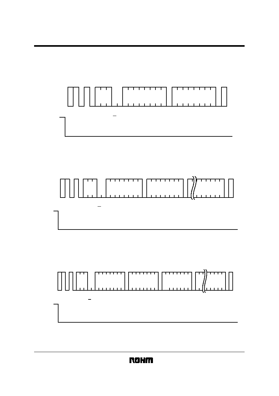
(8) Page write
BR24C08 / F / FJ / FV
1
0
1
0 P2 P1 P0
D7
D0
S
T
O
P
DATA
A
C
K
A
C
K
A
C
K
WORD
ADDRESS
R
/
W
W
R
I
T
E
SLAVE
ADDRESS
S
T
A
R
T
SDA
LINE
WP
Fig.7
WA
7
WA
0
BR24C16 / F / FJ / FV
SDA
LINE
WP
S
T
A
R
T
SLAVE
ADDRESS
1
0
0
1
P2 P1 P0
A
C
K
R
/
W
W
R
I
T
E
WORD
ADDRESS(n)
A
C
K
D7
DATA(n)
DATA(n
+
15)
D0
D0
A
C
K
A
C
K
S
T
O
P
Fig.8
WA
7
WA
0
BR24E16 / F / FJ / FV
SDA
LINE
WP
S
T
A
R
T
SLAVE
ADDRESS
1 0
0
1
A2 A1 A0
A
C
K
R
/
W
W
R
I
T
E
1st WORD
ADDRESS(n)
2nd WORD
ADDRESS(n)
A
C
K
D7
DATA(n)
D0
A
C
K
Fig.9
WA
10
WA
0
DATA(n
+
15)
D0
A
C
K
S
T
O
P
A
C
K
$
A 16 byte write is possible using this command.
$
The page write command arbitrarily sets the upper 4 bits (WA7 to WA4) of the word address.
The lower 4 bits (WA3 and WA0) can write up to 16 bytes of data with the address being incremented internally.
BR24C08 / BR24C08F / BR24C08FJ / BR24C08FV / BR24C16/ BR24C16F /
Memory Ics
BR24C16FJ /
BR24C16FV / BR24E16 / BR24E16F / BR24E16FJ / BR24E16FV
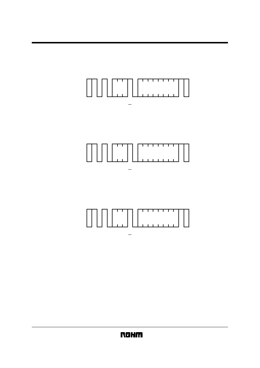
(9) Current read
BR24C08 / F / FJ / FV
SDA
LINE
S
T
A
R
T
SLAVE
ADDRESS
1
1
R
/
W
A
C
K
A
C
K
DATA
S
T
O
P
0
0 A2 P1 P0
D7
D0
R
E
A
D
Fig.10
BR24C16 / F / FJ / FV
SDA
LINE
S
T
A
R
T
SLAVE
ADDRESS
1
1
R
/
W
A
C
K
A
C
K
DATA
S
T
O
P
0
0 P2 P1 P0
D7
D0
R
E
A
D
Fig.11
BR24E16 / F / FJ / FV
SDA
LINE
S
T
A
R
T
SLAVE
ADDRESS
1
1
R
/
W
A
C
K
A
C
K
DATA
S
T
O
P
0
0 A2 A1 A0
D7
D0
R
E
A
D
Fig.12
$
In case the previous operation is random or current read (which includes sequential read respectively), the
internal address counter is increased by one from the last accessed address (n). Thus current read outputs the
data of the next word address (n+1).
If the last command is byte or page write, the internal address counter stays at the last address (n). Thus current
read outputs the data of the word address (n).
If the master does not transfer the acknowledge but does generate a stop condition, the current address read
operation only provides s single byte of data.
At this point, this IC discontinues transmission.
$
When an ACK signal LOW is detected after D0 and a stop condition is not sent from the master (
µ
-COM), the
next word address data can be read.
[
All words all read enabled
]
(See Fig.16 to 18 for the sequential read cycles.)
$
This command is ended by inputting HIGH to the ACK signal after D0 and raising the SDA signal (stop
condition) by setting SCL to HIGH.
BR24C08 / BR24C08F / BR24C08FJ / BR24C08FV / BR24C16/ BR24C16F /
Memory Ics
BR24C16FJ /
BR24C16FV / BR24E16 / BR24E16F / BR24E16FJ / BR24E16FV
(10) Random read
BR24C08 / F / FJ / FV
S
T
O
P
A
C
K
R
E
A
D
DATA(n)
SLAVE
ADDRESS
SLAVE
ADDRESS
WORD
ADDRESS(n)
SDA
LINE
S
T
A
R
T
S
T
A
R
T
1
1
0
0 A2 P1 P0
R
/
W
R
/
W
A
C
K
A
C
K
A
C
K
W
R
I
T
E
1
1
0
0 A2 P1P0
D7
D0
Fig.13
WA
7
WA
0
BR24C16 / F / FJ / FV
S
T
O
P
A
C
K
R
E
A
D
DATA(n)
SLAVE
ADDRESS
SLAVE
ADDRESS
WORD
ADDRESS(n)
SDA
LINE
S
T
A
R
T
S
T
A
R
T
1
1
0
0 P2 P1 P0
R
/
W
R
/
W
A
C
K
A
C
K
A
C
K
W
R
I
T
E
1
1
0
0 P2 P1P0
D7
D0
Fig.14
WA
7
WA
0
BR24E16 / F / FJ / FV
SLAVE
ADDRESS
SDA
LINE
S
T
A
R
T
1
1
0
0 A2 A1 A0
R
/
W
W
R
I
T
E
Fig.15
S
T
O
P
A
C
K
R
E
A
D
DATA(n)
SLAVE
ADDRESS
S
T
A
R
T
R
/
W
A
C
K
A
C
K
1
1
0
0 A2 A1A0
D7
D0
WA
0
1st WORD
ADDRESS(n)
2nd WORD
ADDRESS(n)
A
C
K
WA
10
A
C
K
$
This command can read the designated word address data.
$
When an ACK signal LOW is detected after D0 and a stop condition is not sent from the master (
µ
-COM), the next
word address data can be read.
[
All words all read enabled
]
(See Fig.16 to 18 for the sequential read cycles.)
$
This command is ended by inputting a HIGH signal to the ACK signal after D0 and raising the SDA signal (stop
condition) by raising SCL to HIGH.

BR24C08 / BR24C08F / BR24C08FJ / BR24C08FV / BR24C16/ BR24C16F /
Memory Ics
BR24C16FJ /
BR24C16FV / BR24E16 / BR24E16F / BR24E16FJ / BR24E16FV
(11) Sequential read
BR24C08 / F / FJ / FV
S
T
A
R
T
SLAVE
ADDRESS
R
/
W
A
C
K
A
C
K
A
C
K
A
C
K
R
E
A
D
DATA(n)
DATA(n
+
x)
SDA
LINE
1
1
0
0 A2 P1 P0
D7
D7
D0
D0
S
T
O
P
Fig.16
BR24C16 / F / FJ / FV
S
T
A
R
T
SLAVE
ADDRESS
R
/
W
A
C
K
A
C
K
A
C
K
A
C
K
R
E
A
D
DATA(n)
DATA(n
+
x)
SDA
LINE
1
1
0
0 P2 P1 P0
D7
D7
D0
D0
S
T
O
P
Fig.17
BR24E16 / F / FJ / FV
S
T
A
R
T
SLAVE
ADDRESS
R
/
W
A
C
K
A
C
K
A
C
K
A
C
K
R
E
A
D
DATA(n)
DATA(n
+
x)
SDA
LINE
1
1
0
0 A2 A1 A0
D7
D7
D0
D0
S
T
O
P
Fig.18
$
When an ACK signal LOW is detected after D0 and a stop condition is not sent from the master (
µ
-COM), the
next word address data can be read.
[
All words can be read
]
$
This command is ended by inputting a HIGH signal to the ACK signal after D0 and raising the SDA signal (stop
condition) using the SCL signal HIGH.
$
Sequential reading can also be done with a random read.
BR24C08 / BR24C08F / BR24C08FJ / BR24C08FV / BR24C16/ BR24C16F /
Memory Ics
BR24C16FJ /
BR24C16FV / BR24E16 / BR24E16F / BR24E16FJ / BR24E16FV
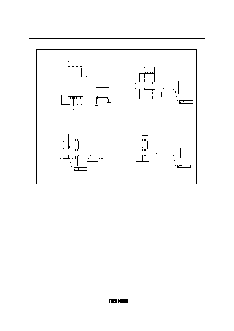
External dimensions (Units : mm)
DIP8
0.5
±
0.1
3.2
±
0.2
3.4
±
0.3
8
5
1
4
9.3
±
0.3
6.5
±
0.3
0.3
±
0.1
0.51Min.
2.54
0
∞
~15
∞
7.62
BR24C08
BR24C16
BR24E16
SOP8
0.15
0.3Min.
0.15
±
0.1
0.4
±
0.1
0.11
6.2
±
0.3
4.4
±
0.2
5.0
±
0.2
8
5
4
1
1.27
1.5
±
0.1
BR24C08F
BR24C16F
BR24E16F
SSOP-B8
5
4
8
1
0.1
6.4
±
0.3
4.4
±
0.2
3.0
±
0.2
0.22
±
0.1
1.15
±
0.1
0.65
(0.52)
0.15
±
0.1
0.3Min.
0.1
BR24C08FV
BR24C16FV
BR24E16FV
BR24C08FJ
BR24C16FJ
BR24E16FJ
SOP-J8
0.1
0.45Min.
0.42
±
0.1
4.9
±
0.2
8
5
4
1 2 3
1.27
7 6
0.2
±
0.1
0.175
6.0
±
0.3
3.9
±
0.2
1.375
±
0.1