EMT2 / EMT3 / UMT2N / IMT2A / IMT3A
Transistors
General purpose (dual transistors)
EMT2 / EMT3 / UMT2N / IMT2A / IMT3A
!
Features
1) Two 2SA1037AK chips in a EMT or UMT or SMT package.
!
Equivalent circuits
(1)
(2)
(3)
(4) (5)
(6)
(6)
(5)
(4)
(3) (2)
(1)
(1)
(2)
(3)
(4)
(5)
(6)
(6)
(5)
(4)
(3)
(2)
(1)
EMT2 / UMT2N
IMT2A
IMT3A
EMT3
!
Absolute maximum ratings (Ta=25
�C)
Parameter
Symbol
V
CBO
V
CEO
V
EBO
I
C
P
C
Tj
Tstg
Limits
-
60
-
50
-
6
150
300(TOTAL)
150(TOTAL)
EMT2 / EMT3 / UMT2N
IMT2A / IMT3A
150
-
55
~
+
150
Unit
V
V
V
mA
mW
�
C
�
C
Collector-base voltage
Collector-emitter voltage
Emitter-base voltage
Collector current
Collector power
dissipation
Junction temperature
Storage temperature
1 120mW per element must not be exceeded.
2 200mW per element must not be exceeded.
1
2
!
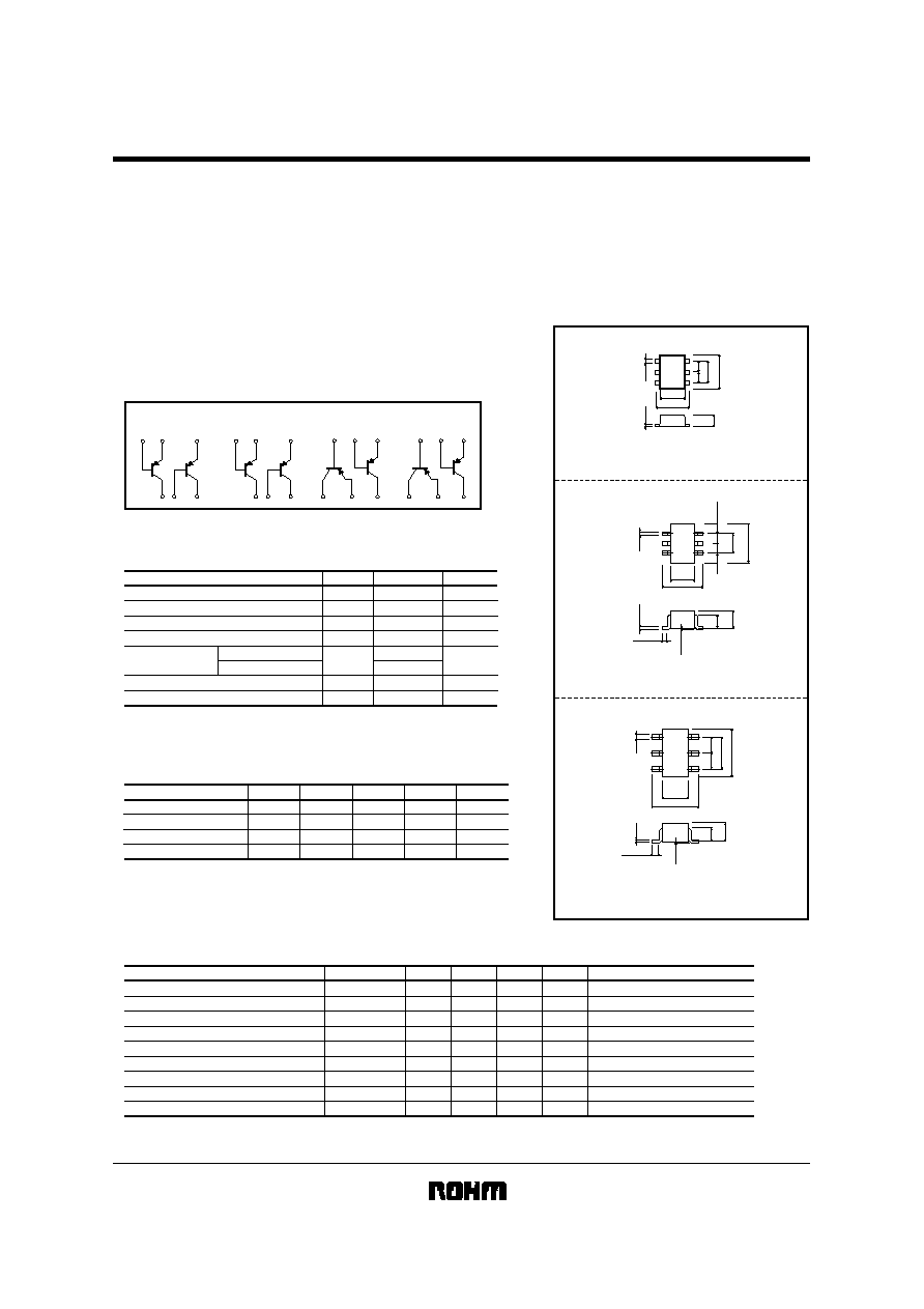
Package, marking, and packaging specifications
EMT2
EMT6
T2
T2R
8000
EMT3
EMT6
T3
T2R
8000
IMT2A
SMT6
T2
T108
3000
IMT3A
SMT6
T3
T108
3000
UMT2N
UMT6
T2
TR
3000
Type
Package
Marking
Code
Basic ordering unit (pieces)
!
External dimensions (Units : mm)
ROHM : EMT6
EMT2 / EMT3
ROHM : UMT6
EIAJ : SC-88
UMT2N
ROHM : SMT6
EIAJ : SC-74
IMT2A / IMT3A
0.22
1.2
1.6
(1)
(2)
(5)
(3)
(6)
(4)
0.13
0.5
0.5
0.5
1.0
1.6
Each lead has same dimensions
0.1Min.
0~0.1
( 6
)
2.0
1.3
0.9
0.15
0.7
2.1
0.65
0.2
1.25
( 1
)
0.65
( 4
)
( 3
)
( 2
)
( 5
)
Each lead has same dimensions
( 6
)
( 5
)
( 4
)
0.3Min.
0.15
0.3
1.1
0.8
0~0.1
( 3
)
2.8
1.6
1.9
2.9
0.95
( 2
)
0.95
( 1
)
Each lead has same dimensions
!
Electrical characteristics (Ta=25
�C)
Parameter
Symbol
Min.
Typ.
Max.
Unit
Conditions
Transition frequency
BV
CBO
BV
CEO
BV
EBO
I
CBO
I
EBO
V
CE(sat)
h
FE
f
T
-
60
-
50
-
6
-
-
-
120
-
-
-
-
-
-
-
-
140
-
-
-
-
0.1
-
0.1
-
0.5
560
-
V
V
V
�
A
�
A
V
-
MHz
Cob
-
4
5
pF
I
C
=-
50
�
A
I
C
=-
1mA
I
E
=-
50
�
A
V
CB
=-
60V
V
EB
=-
6V
V
CE
=-
12V, I
E
=
2mA, f
=
100MHz
V
CE
=-
12V, I
E
=
0A, f
=
1MHz
I
C
/I
B
=-
50mA/
-
5mA
V
CE
=-
6V, I
C
=-
1mA
Transition frequency of the device.
Collector-base breakdown voltage
Collector-emitter breakdown voltage
Emitter-base breakdown voltage
Collector cutoff current
Emitter cutoff current
Collector-emitter saturation voltage
DC current transfer ratio
Output capacitance