IA2004-CE10A
Contact image sensor heads
1/4
Image sensor heads for narrow-width scanners
IA2004-CE10A
Equipped with the sensor chips that have built-in analog memory, this compact color image sensor head is suitable for
any scanning application that requires raped scanning of widths of up to A6. It best fits into the photo graphic applications.
Applications
Check readers, card scanners, and a variety of other image input devices.
Features
1) By integrating the signal amplifier on the sensor chip, external noise is shut out. Additionally, newly developed analog
memory circuit and realizes high speed scanning.
2) The LED light source is mounted on the same substrate as the sensor chip which makes it possible to package the
device with lighter weight and an extremely small size.
3) With the proprietary prism(reflectors), the output signal is maintained uniformly.
4) The ceramic substrate is used for excellent dimensional accuracy and thermal stability.
Variation and maximize the image re-productivity.
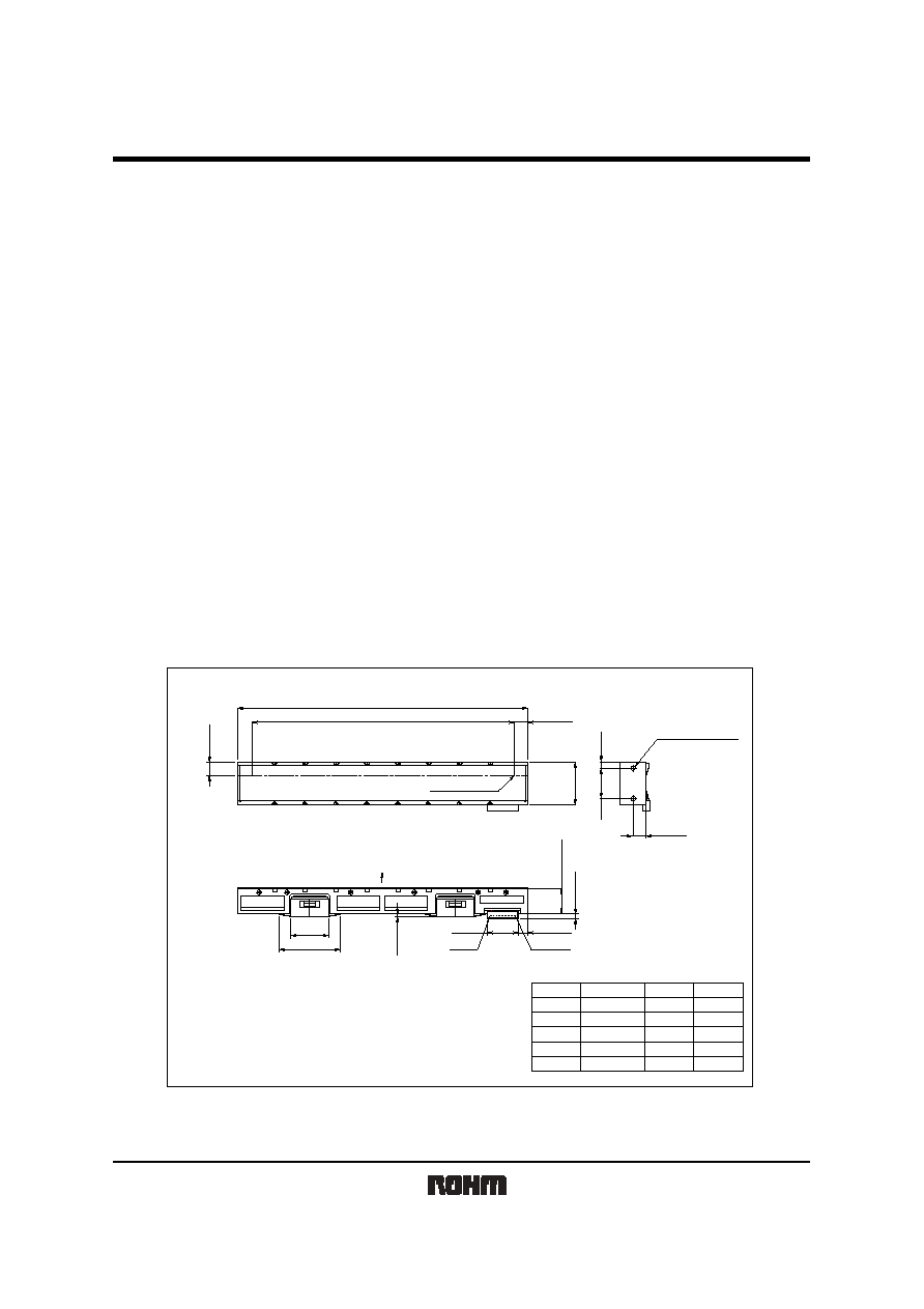
External dimensions (Unit : mm)
2.5
(12.9)
Max. 1.5
108(Effective Reading Width:101.6)
(3.8)
Max.2
Pin No.
Pin No.
Signal
Signal
No.1
No.2
No.3
No.4
No.5
No.6
No.7
Ao
GND
SI
CLK
V
DD
RLED
GLED
A
L
C
No.9
No.1
No.1 Pixel
No.8
No.9
BLED
VLED
Note) Deflection at the top of glass : 0 to 0.25
Projection to platen is positive
Socket Housing : IL-Z-9S-S125C3(JAE)
Socket Contact : IL-Z-C3-A-15000(JAE)
119.5 0.3
+
-
0.25
17.5
+ -
12.5 0.05
+-
25 1
+
-
15.5 1
+
-
5 0.1
+
-
2 0.05
+
-
10.36 0.4
+ -
0.3
5.5
+
-
(5.5 )
Depth1

Appendix
Appendix1-Rev1.1
The products listed in this document are designed to be used with ordinary electronic equipment or devices
(such as audio visual equipment, office-automation equipment, communications devices, electrical
appliances and electronic toys).
Should you intend to use these products with equipment or devices which require an extremely high level of
reliability and the malfunction of with would directly endanger human life (such as medical instruments,
transportation equipment, aerospace machinery, nuclear-reactor controllers, fuel controllers and other
safety devices), please be sure to consult with our sales representative in advance.
Notes
No technical content pages of this document may be reproduced in any form or transmitted by any
means without prior permission of ROHM CO.,LTD.
The contents described herein are subject to change without notice. The specifications for the
product described in this document are for reference only. Upon actual use, therefore, please request
that specifications to be separately delivered.
Application circuit diagrams and circuit constants contained herein are shown as examples of standard
use and operation. Please pay careful attention to the peripheral conditions when designing circuits
and deciding upon circuit constants in the set.
Any data, including, but not limited to application circuit diagrams information, described herein
are intended only as illustrations of such devices and not as the specifications for such devices. ROHM
CO.,LTD. disclaims any warranty that any use of such devices shall be free from infringement of any
third party's intellectual property rights or other proprietary rights, and further, assumes no liability of
whatsoever nature in the event of any such infringement, or arising from or connected with or related
to the use of such devices.
Upon the sale of any such devices, other than for buyer's right to use such devices itself, resell or
otherwise dispose of the same, no express or implied right or license to practice or commercially
exploit any intellectual property rights or other proprietary rights owned or controlled by
ROHM CO., LTD. is granted to any such buyer.
Products listed in this document are no antiradiation design.
About Export Control Order in Japan
Products described herein are the objects of controlled goods in Annex 1 (Item 16) of Export Trade Control
Order in Japan.
In case of export from Japan, please confirm if it applies to "objective" criteria or an "informed" (by MITI clause)
on the basis of "catch all controls for Non-Proliferation of Weapons of Mass Destruction.


