
IA6008-FB10A
Contact image sensor heads
1/5
Color image sensor heads for multi-function
IA6008-FB10A
"Color contact image sensor" with optical system intended for Flatbed scanning. Optical technology established for
sheet-feed scanning has been further advanced for Flatbed scanning. Furthermore, a newly developed sensor with
resolution selection function provides more freedome in choosing the adequate optical resolution matching to the
application.
Applications
Image sensor heads device for multiple function facsimiles such as color scanner and multiple function printer.
Features
1) Signal amplifier is built in to the image sensor IC in order to increase immunity to external noise.
2) A low-voltage drive sensor is employed, which runs at 3.3V like ASIC
3) The LED light source is mounted on the same substrate as the sensor chip which makes it possible to package the
device with lighter weight and an extremely small size.
4) With the proprietary prism, the output signal is maintained uniformly.
5) The ceramic substrate is used for excellent dimensional accuracy and thermal stability.
External dimensions (Unit : mm)
Pin No.
Signal
No.1
No.2
No.3
No.4
No.5
No.6
Ao
MODE
GND
V
DD
V
REF
SP
Pin No.
Signal
No.7
No.8
No.9
No.10
No.11
No.12
CLK
V-LED
B-GND
G-GND
R-GND
NC
6.9
236
±
0.5
2
±
0.2
14
±
0.2
2
-
1.5x2
Oval Hole D4MIN
2
-
1.5 D4MIN
2
-
3
0.324
±
0.1
14
±
0.2
6.9
17.5
max.1
max.1
max.1
max.1
15
13.8
9.4
MAX 3.15
+
0
-
0.05
No.12
No.1
+
+
Scanning Line
216 (Effective Reading With)
Effective 1st bit
1mm pitch 12pin
Center of FCC

IA6008-FB10A
Contact image sensor heads
3/5
Timing chart
(a) CLK
Timing
Chart
ts
tHOLD
tSETUP
twH
1/fCLK
CLK
twL
SP
Ao
1pixel
2pixel
50%
50%
(b) Data Output Timing Chart (600dpi mode)
After turning on the SP pulse, the analog output starts from the setting up point of 64 clock pulse.
Note)The CLK section area which is over the effective pixel numbers
(Output blank part) cannot be used as the analog Output
standard level.
CLK
1
SP
Ao
2
82
83
84
136 137 138
Vref output period(52pixels)
Vdummy
Analog output period
1 to 82pixels
83 to 136pixels
137 to 5266pixels
IA6008-FB10A
Contact image sensor heads
4/5
Data Output Timing Chart (300dpi mode)
After turning on the SP pulse, the analog output starts from the setting up point of 64 clock pulse.
Note)The CLK section area which is over the effective pixel numbers
(Output blank part) cannot be used as the analog Output
standard level.
CLK
1
SP
Ao
2
82
83
84
109 110 111
Vref output period(52pixels)
Vdummy
Analog output period
1 to 82pixels
83 to 109pixels
110 to 2674pixels
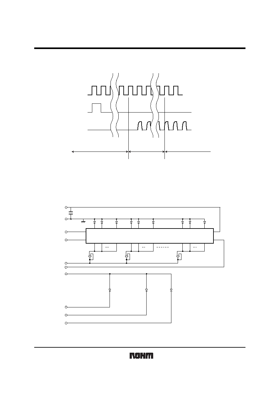
Circuit diagram
V
DD
GND
SP
CLK
A
O
ANALOG MEMORY CIRCUIT
5184
1
V
LED
V
REF
V
DD
V
REF
R
GND
G
GND
B
GND
1
µ
F
◊
3

