KF2004-GM50A
Printheads
Thick film thermal printhead
(with thermal historical control)
KF2004-GM50A
GM50 series is the new product that newly added the future history control and driver LSI which has the function of
thermal historical control, to GL50 series which is employing the convertional thick-film fast response thermal element.
!
!
!
!
Applications
High speed label printer
High speed bar code printer
High speed ticket printer
Various high speed terminal printers
!
!
!
!
Features
1) Newly developed thick-film fast response thermal element and driver LSI with the function of thermal history control
which is added the future history control are employed for this series. It is possible to print with super high speed of 10
inches / s or 250mm / s.
2) 150km life realized by attributing durable new protection film.
3) New partial glaze construction makes it compatible with the thermal transfer application.
4) Market-proven G-series printhead construction ensures high reliability.
!
!
!
!
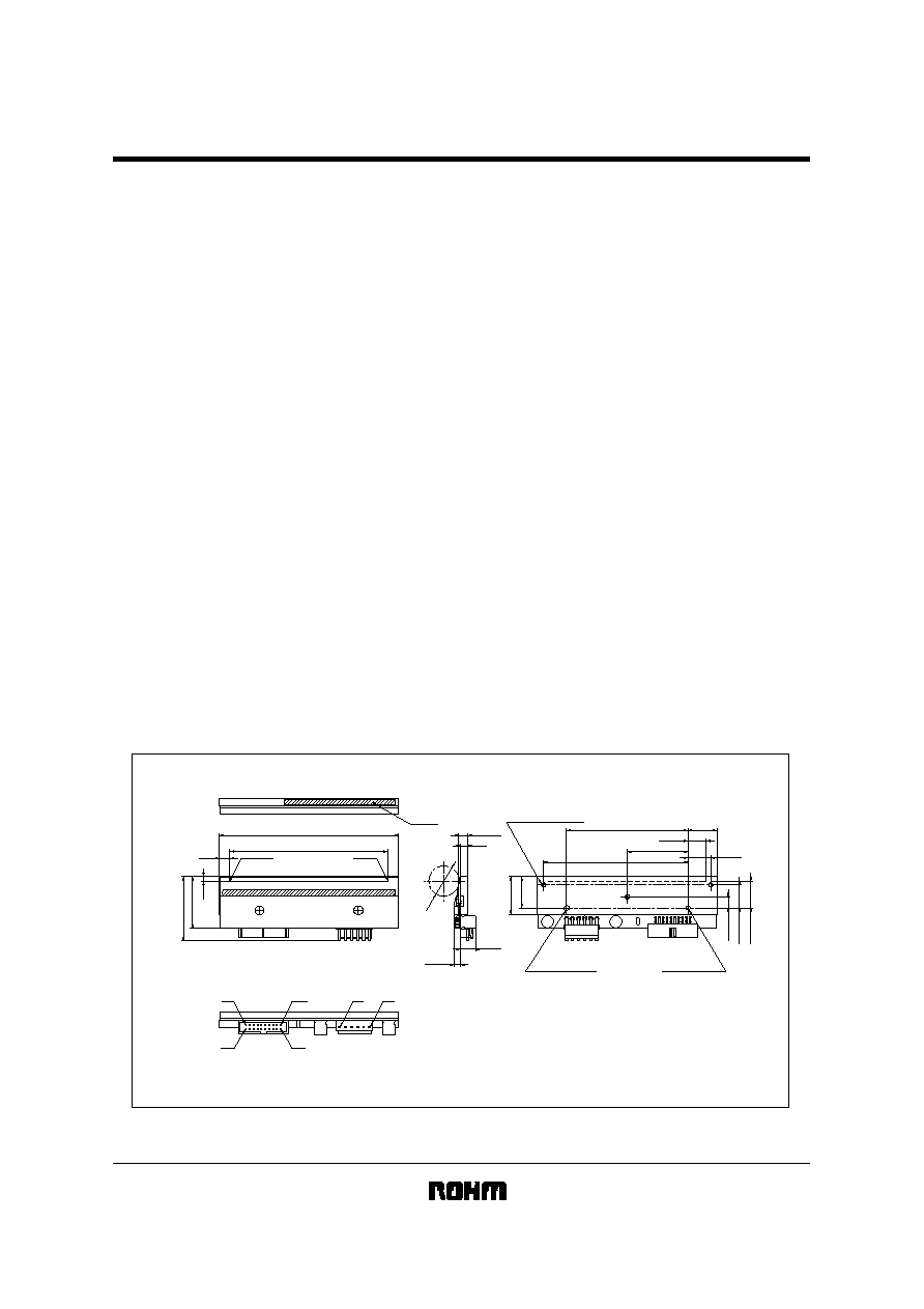
External dimensions (Units : mm)
20
Max.12
(7)
12
±0.2
40
±0.3
Dot #1
Max.45
Dot #832
104 (Effective Print Width)
LABEL
Max.5.5
(5)
6.1±0.4
15±0.3
17.8±0.2
7.3±0.3
15.3±0.3
80±0.3
95±0.3
(20.8)
25±0.5
118
(3)
Max.36
(19)
3-M3 (Effective Depth 3)
3H10 Length 4
(Effective Depth 3)
3H10
(Effective Depth 3)
#1
#6
#20
#19
CONNECTOR B
#1
#2
CONNECTOR A
KF2004-GM50A
Printheads
!
!
!
!
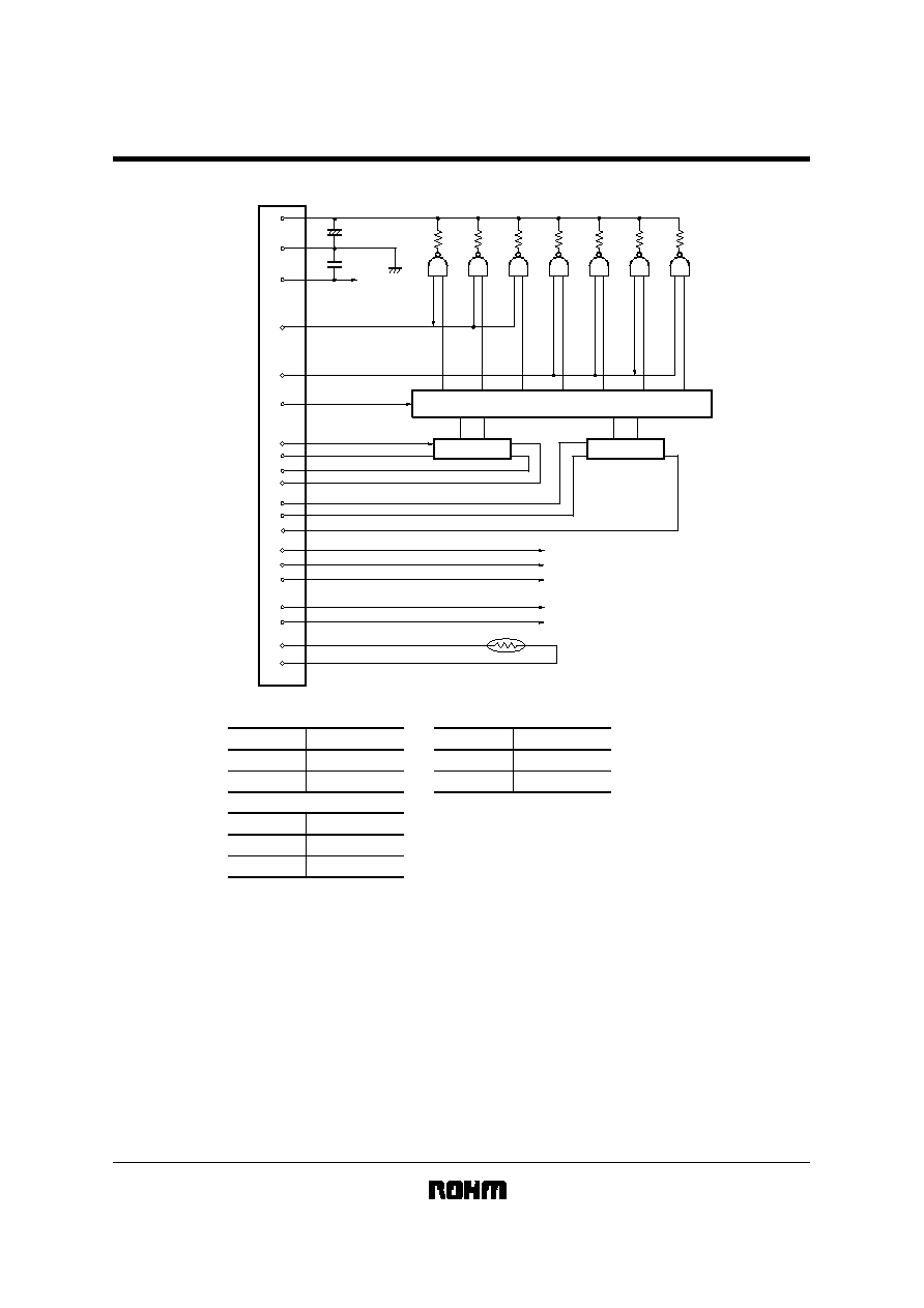
Pin assignments
/ RESET
START
DO1
DO2
TM
TM
/ STB2
/ STB1
CLKOUT2
CLKIN1
V
H
(COM)
V
H
(COM)
V
H
(COM)
GND
GND
GND
11
12
13
14
15
16
17
18
19
20
No.
Circuit
No.
1
2
3
4
5
6
Circuit
V
DD
V
DD
SEL2
SEL1
CLKIN2 (CP)
NC
DI2
DI1
INC
/ LOAD
No.
1
2
3
4
5
6
7
8
9
10
Circuit
CONNECTOR A
CONNECTOR B
!
!
!
!
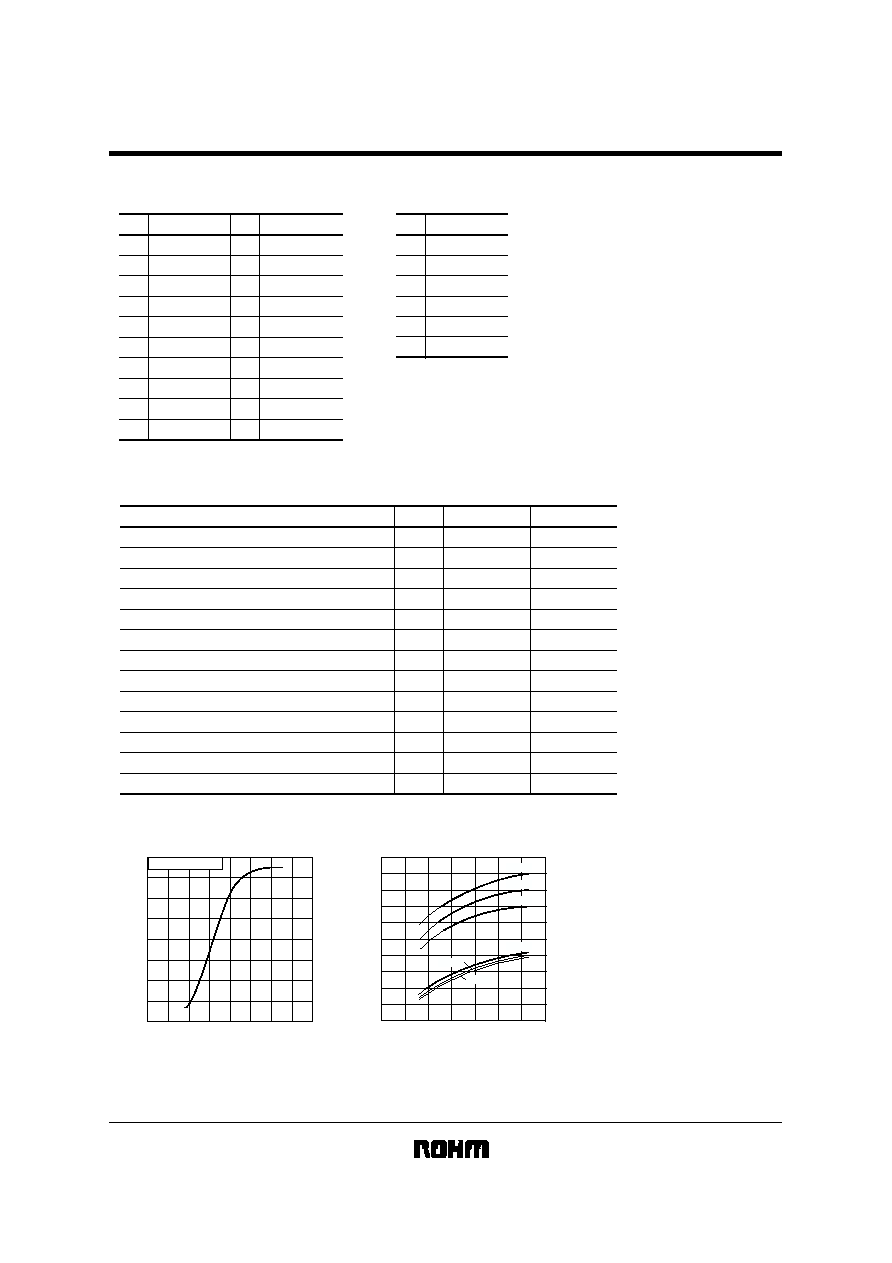
Characteristics
Parameter
-
Rave
V
H
P
O
104
0.125
832
550
24
0.857
0.490
0.258
832
8
20.0
-
-
SLT
T
ON
-
-
mm
mm
dots
V
W/dot
ms
ms
dots
MHz
mm
-
150/(1
×
10
8
)
5~45
-
-
km/pulses
°
C
Effective printing width
Symbol
Typical
Unit
Average resistance value
Dot pitch
Total dot number
Pulse width
Maximum number of dots energized simultaneously
Maximum clock frequency
Maximum roller diameter
Running life / pulse life
Operating temperature
Applied power
Applied voltage
Print cycle
!
!
!
!
Data sheets
ENERGY (mJ/dot)
Fig.2 Representative density curve
OPTICAL DENSITY
SLT : 0.82ms / line
0.40
0.30 0.35
0.20 0.25
0.10 0.15
1.6
1.4
1.2
1.0
0.8
0.6
0.4
0.2
0
0.00 0.05
SCANNING LINE TIME (ms/line)
Fig.3 Maximum energy curve
MAXIMUM ENERGY (mJ/dot)
0
0.4
0.2
0.8
1.0
0.6
1.2
1.4
1.0
0.9
0.8
0.7
0.6
0.5
0.4
0.3
0.2
0.1
0.0
Level1
Level2
Level3
Level4
Level5
Level6