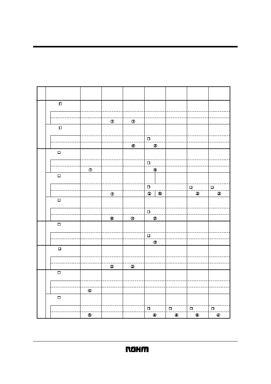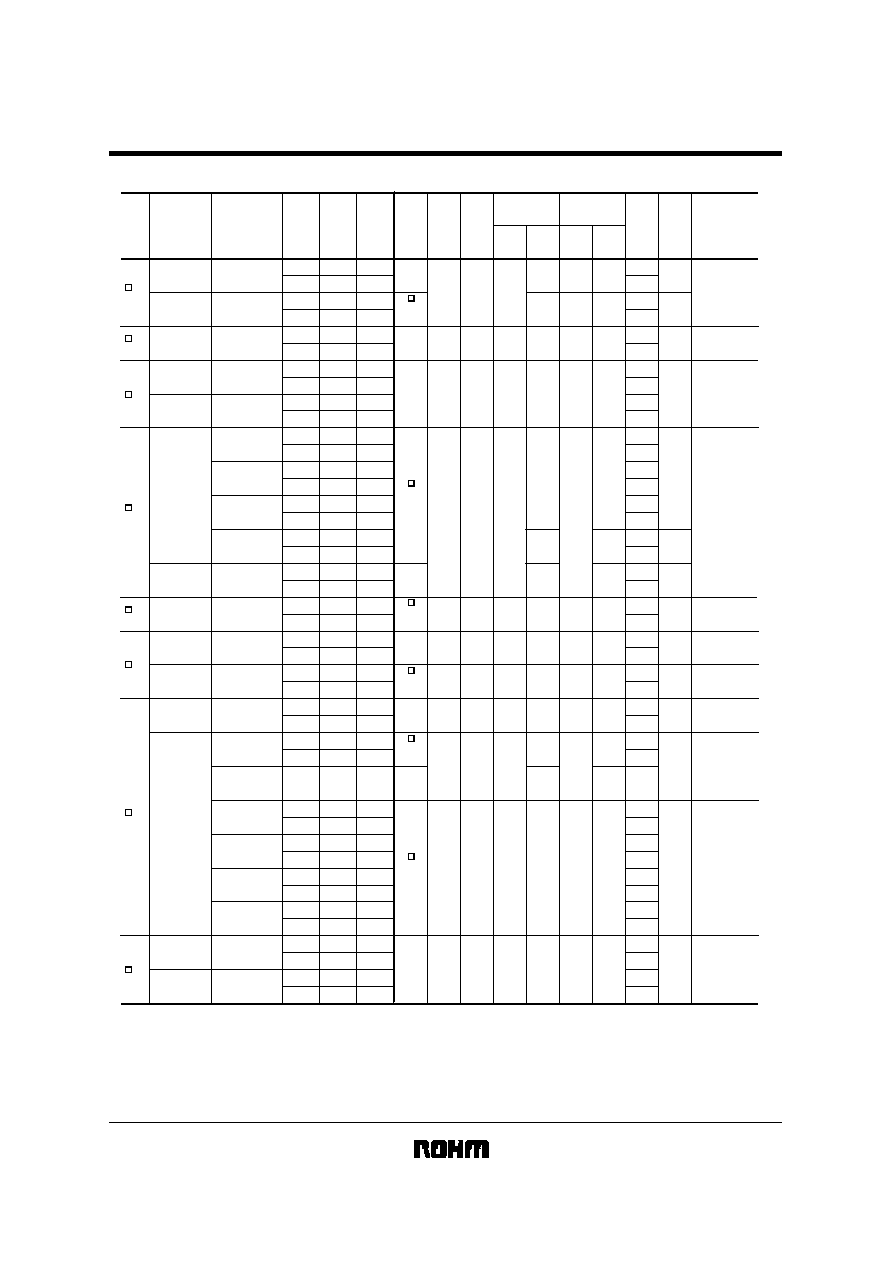
LUM unit series
LED displays
!
!
!
!
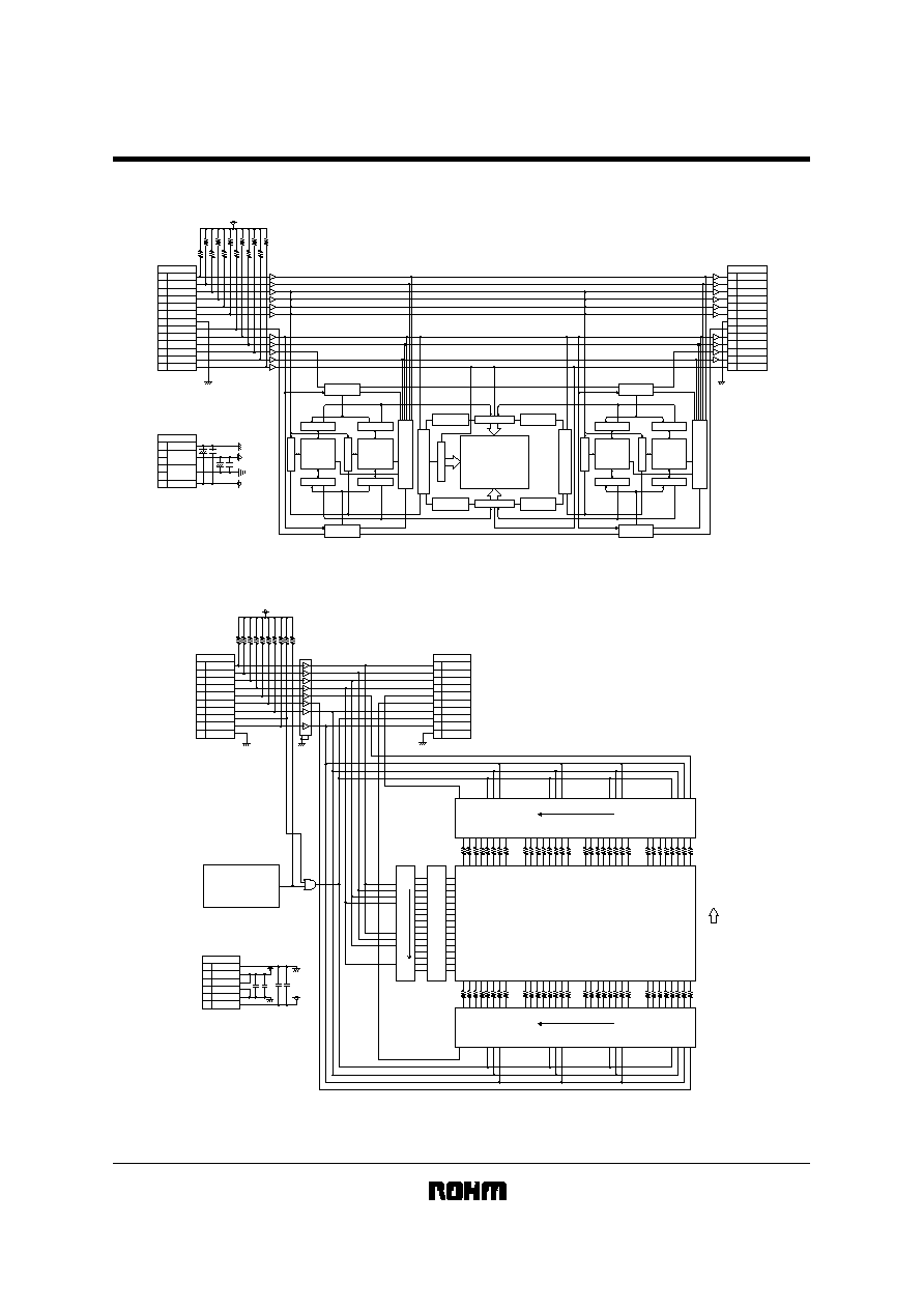
Block diagrams
(1) Memory Type (LUM-512HML300 is advertised in here for just memory type of an example)
5
3
1
GND
2
VLED
4
GNDLED
6
VDD
CN-3
TIMING CONTROLLER
BRIGHT
CONTROLLER
BRIGHT
CONTROLLER
ADDRESS DECODER
DATA BUFFER
16
×
16
RED&GREEN
RAM A
DATA BUFFER
GREEN 16bit
SHIFT RESISTER
DATA BUFFER
RAM B
RED&GREEN
16
×
16
DATA BUFFER
ADDRESS DECODER
MEMORY CONTROLLER
RED 16bit
SHIFT RESISTER
SHIFT RESISTER
RED 16bit
CONTROLLER
BRIGHT
CONTROLLER
BRIGHT
LED MATRIX
16
×
32
GREEN DRIVER
RED DRIVER
COMMON DRIVER
TIMING CONTROLLER
MEMORY CONTROLLER
ADDRESS DECODER
DATA BUFFER
16
×
16
RED&GREEN
RAM B
DATA BUFFER
SHIFT RESISTER
GREEN 16bit
DATA BUFFER
RAM A
RED&GREEN
16
×
16
DATA BUFFER
ADDRESS DECODER
12
SEout
11
A/BBout
10
A3out
9
A2out
8
A1out
7
A0out
6
GND
5
GRout
4
CLKout
3
WEout
2
RDout
1
AEout
13
ENBout
CN-2
4.7k
×
12
CN-1
ENBin
13
AEin
12
RDin
11
WEin
10
CLKin
9
GRin
8
GND
7
A0in
6
A1in
5
A2in
4
A3in
3
A/BBin
2
SEin
1
(2) Shift register type (LUM-512HML320 is advertised in here for just shift register type of an example)
5
3
1
GND
2
VLED
VLED
4
LEDGND
LEDGND
6
VDD
CN3
+
+
-
-
A0
A15
RED 32bit SHIFT RESISTER
direction of data shift
GREEN 32bit SHIFT RESISTER
direction of data shift
LED MATRIX
TEMPERATURE
OBSERVATION
UP
Front view of
display part
ANODE COMMON DRIVER
DECODE
16
×
32
4.7k
×
1.0
CN1
GND
10
CLKin
9
ENBin
8
LATCHin
7
Grnin
6
Redin
5
A3in
4
A2in
3
A1in
2
A0in
1
CN2
GND
1
CLKout
2
ENBout
3
LATCHout
4
Grnout
5
Redout
6
A3out
7
A2out
8
A1out
9
A0out
10

LUM unit series
LED displays
!
!
!
!
Pin descriptions
(1) CN-1
1) RDin
Data input for red LED. LED is on when this pin is HIGH, and off when it is LOW.
2) GRin
Data input for green LED. LED is on when this pin is HIGH, and off when it is LOW.
3) CLKin
Clock input. Used to load RDin and GRin data. Data is loaded into the internal shift registor at the leading edge of the CLK
signal.
4) A0in - A3(A4)in
RAM address input. This specifies the address in memory to which display data will be written.
5) WEin
Write control signal. When this signal is HIGH, the contents of the internal shift registor are written to memory.
(Only valid when AEin is HIGH.)
6) AEin
Address control signal. When this signal is HIGH, the current address in A0in - A3(A4)in is specified.
7) A/ BBin
Control signal for selecting memory where data will be written. When this signal is HIGH, ARAM is selected, and when it is
LOW, BRAM is selected. (Only valid when SEin is HIGH.) The contents of the memory not selected for writing will be
displayed.
8) SEin
This signal determines whether memory selection will be made by external control or internal control. When this signal is
HIGH, the A/ BBin signal determines whether ARAM or BRAM is selected. When ARAM is selected for writing, the BRAM
data is displayed, and when BRAM is selected for writing, the ARAM data is displayed. When this signal is LOW, data will
be written to a different memory (from address 0) after the last memory address (15 or 23) is written to. The display data
will change simultaneously with the memory change.
9) ENBin
Display output is Enable. It becomes display state HIGH level, non-display state at Low level.
(2) CN-2
1) RDout
Data output for red LED. The signal is output simultaneously with CLK after passing through internal bit shift register 16
(24, 32, 48). If LED modules are connected serially, this pin will be connected to the next module's RDin pin.
2) GRout
Data output for green LED. The signal is output simultaneously with CLK after passing through internal bit shift register 16
(24, 32, 48). If LED modules are connected serially, this pin will be connected to the next module's RDin pin.
3) CLKout
Clock signal output. This pin outputs the CLKin signal. The pin connects to the next module's CLKin pin.
4) A0out - A3(A4)out
Address signal output. These pins output the signals of A0in - A3(A4)in. The pins connect to the next module's A0in -
A3(A4)in pins.
5) WEout
WE (write control) signal output. This pin outputs the WEin signal. The pin connects to the next module's WEin pin.
6) AEout
AE (address control) signal output. This pin outputs the AEin signal. The pin connects to the next module's AEin pin.
7) A/BBout
A/BB (selection of memory for writing) signal output. This pin outputs the A/BBout signal. The pin connects to the next
module's A/BBin pin.
8) SEout
SE (memory selection control) signal output. This pin outputs the SEin signal. The pin connects to the next module's SEin
pin.
LUM unit series
LED displays
9) ENBout
ENB signal output. The ENBin signal is outputted. It is connected to ENBin of the next module.
!
!
!
!
Shift register type pin function specifications
-CN1-
·CLKin
Clock input. Used to load RDin and GRin data. Data is loaded into the internal shift registor at the leading edge
of the CLK signal.
·Redin
Data input for red LED. LED is on when this pin is HIGH, and off when it is LOW.
·Gmin
Data input for green LED. LED is on when this pin is HIGH, and off when it is LOW.
·LATCHin Inputs a display data latch signal. The data is latched at Low and put through at High.
·ENBin
Inputs a display enable signal. The display turns OFF at High and turns ON at Low.
·A0~A3in Inputs a common selection address signal. Specifies the common address in which the display data is output.
ACOM0
ACOM1
ACOM2
ACOM3
ACOM4
ACOM5
ACOM6
ACOM7
ACOM8
ACOM9
ACOM10
ACOM11
ACOM12
ACOM13
ACOM14
ACOM15
A0
0
1
0
1
0
1
0
1
0
1
0
1
0
1
0
1
A1
0
0
1
1
0
0
1
1
0
0
1
1
0
0
1
1
A2
0
0
0
0
1
1
1
1
0
0
0
0
1
1
1
1
A3
0
0
0
0
0
0
0
0
1
1
1
1
1
1
1
1
·GND
Control circuit ground.
-CN2-
·CLKout Clock signal output. This pin outputs the CLKin signal. The pin connects to the next module's CLKin pin.
·Redout Data output for red LED. The signal is output simultaneously with CLK after passing through internal bit shift
register 16 (24, 32, 48). If LED modules are connected serially, this pin will be connected to the next module's
RDin pin.
·Gmout
Data output for green LED. The signal is output simultaneously with CLK after passing through internal bit shift
register 16 (24, 32, 48). If LED modules are connected serially, this pin will be connected to the next module's
GRin pin.
·LATCHout Outputs a display data latch signal. An LATCHin signal is output. Connect this to the next module's LATCHin.
·ENBout Outputs a display enable signal. An ENBin signal is output. Connect this to the next module's ENBin.
·A0~A3out Outputs a common selection address. An A0in-A3in signal is output. Connect this to the next module's A0in-
A3in.
·GND
Ground for the control circuit.