Äîêóìåíòàöèÿ è îïèñàíèÿ www.docs.chipfind.ru
RCM2228R-A / B
Liquid Crystal Displays
1/7
16 characters
×
2 lines COG module
RCM2228R-A / B
The RCM2228R-A / B is a reflective TN type liquid crystal module with a built-in controller / driver LSI and a display
capacity of 16 characters
×
2 lines.
Applications
Printers, Copiers, Facsimiles, etc
Features
(1) 5
×
7 dot character matrix with cursor.
(2) Interfaces with 4-bit MPUs.
(3) Displays up to 237 characters and special symbols.
(4) Custom character patterns are displayed with the character RAM.
(5) Abundant instruction set including clear display, cursor on/off, and character blinking.
(6) Compact and lightweight for easy assembly to the host instrument.
(7) Operable on single 5V power supply.
(8) Low power consumption.
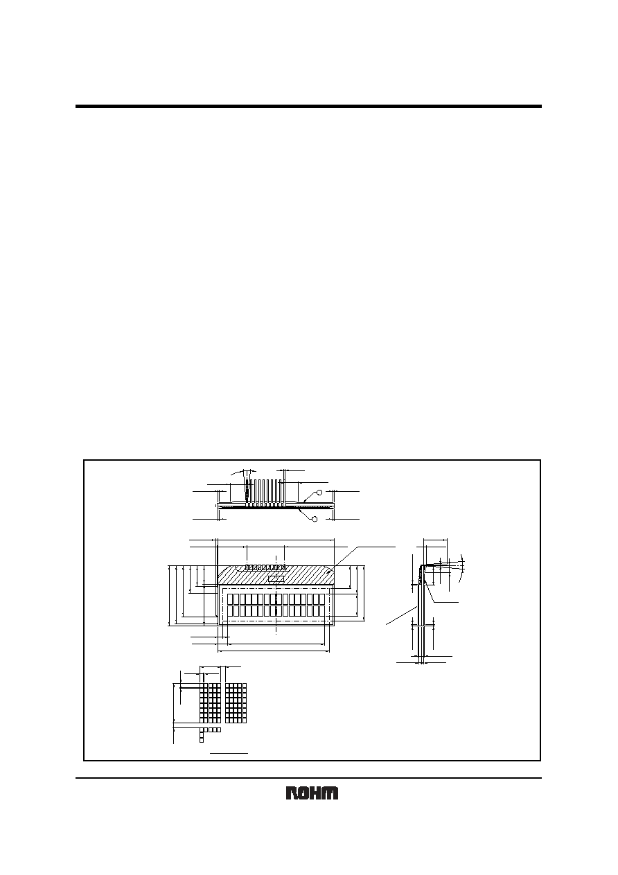
External dimensions (Unit : mm) (Viewing direction : 6 : 00)
12.4
±
0.3
No.1
No.10
50.0
±
0.3
0.3MAX.
1.0MAX.
2.0MAX.
41.9
±
0.2
48.0MIN.
10.0MAX.
9.4
±
0.2
12.3
±
0.3
24.0MIN.
1
2
(0.5)
±
5
°
8.0
±
0.3
(18.0)
9.0MIN.
12.0MIN.
22.0MAX.
25.0MAX.
26.0
±
0.3
2.7
±
0.3
±
5
°
0.39
2.15
0.5
0.5
4.35
0.7
0.7
±
0.7
0.7
±
0.7
0.7
±
0.7
0.7
±
0.7
0.7
±
0.7
0.7
±
0.7
0.7
±
0.7
8.7
±
0.7
Shield tape
Over-coating regin
10.0
±
0.5
Dot de tail
7.0MAX
6.0MAX
Viewing direction
6:00
(PITCH1.8
×
9)16.2
±
0.3
1.1
±
0.1
1.1
±
0.1
(0.3)
0.05
0.05
4.0MAX
1.5MAX
4.05
±
0.3
RCM2228R-A / B
Liquid Crystal Displays
2/7
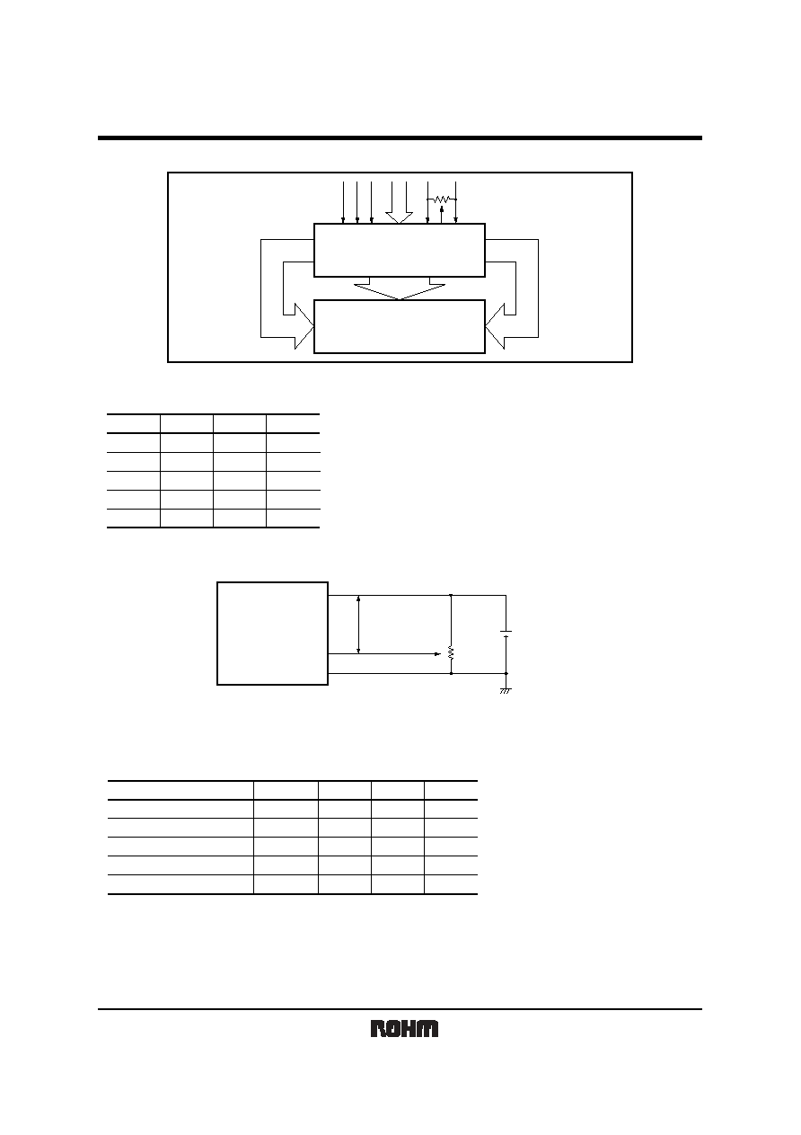
Block diagram
SEG1~80
16character
×
2lines
COM
1~8
COM
9~16
V
D
D
V
S
S
V
0
R
S
R
/
W
E
D
B
4
~
D
B
7
V
R
Pin assignments
Symbol
Symbol
Pin No.
1
2
3
4
5
Pin No.
RS
R / W
6
DB6
E
7
DB7
DB4
8
V
SS
DB5
9
V
DD
10
V
0
Power supply example
LCD MODULE
V
DD
V
DD
-
V
0
V
DD
-
V
0
: LCD drive voltage
V
DD
V
R
V
0
V
SS
Fig.1
Absolute maximum ratings (Ta=25
°
C)
Parameter
Min.
-
0.3
-
0.3
-
0.3
0
Symbol
V
DD
V
LCD
V
IN
Topr
Tstg
Max.
6.0
6.0
V
DD
+
0.3
50
70
Unit
V
V
V
°
C
°
C
-
20
Power voltage for logics
Power voltage for driving LCD
Input voltage
Operating temperature
Storage temperature
RCM2228R-A / B
Liquid Crystal Displays
3/7
Electrical characteristics (V
DD
=5.0V, Ta=25
°
C)
Parameter
Symbol
V
DD
V
LCD
V
IH
V
IL
fosc
Min.
4.75
3.0
0.7V
DD
V
SS
-
0.3
0.75V
DD
Typ.
5.0
0.5
Max.
5.25
5.0
V
DD
0.6
0.2V
DD
1.0
1100
Unit
V
V
V
V
V
V
mA
Conditions
V
DD
=
5.0V, fosc=270kHz check pattem
RS, R / W, CS
-
-
-
-
-
-
V
SS
kHz
540
350
-
Logic power voltage
LCD driving voltage
"H" input voltage
"L" input voltage
"H" output voltage
"L" output voltage
Clock frequency
Current consumption
IOH
= -
0.1mA
IOL
=
0.1mA
V
OH
V
OL
I
DD
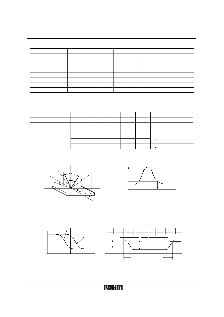
Optical characteristics (Ta=25
°
C)
When viewing from below
Parameter
Symbol
t
r
t
d
K
1
2
Min.
-
-
-
-
40
±
30
Typ.
100
150
3.0
-
-
-
Max.
250
250
-
10
-
-
Unit
ms
ms
-
deg
deg
deg
Conditions
=
0
°
,
=
10
°
K 1.4,
=
0
°
K 1.4,
=
10
°
=
0
°
,
=
10
°
=
0
°
,
=
10
°
Response time
Response time
Contrast ratio
Viewing angle
>
>
90%
100%
10%
t
r
t
d
100
0
B
1
B
2
K=B
2
/ B
1
1.4
1
2
Viewing direction
12 o'clock
Viewing direction 6 o'clock
X
X'
2
2'
1
1'
Y (
=
180
°
)
Y' (
=180
°
)
Z (
=0
°
)
Fig.2
Fig.4
Fig.3
Fig.5
Selected condition
Rise time
Fall time
Non-selected
Selected
Brightness (%)
Driving voltage
Viewing angle
Contrast ratio
(1) Definition
and
(3) Definition of contrast ratio "K"
(2) Definition of viewing angles
1 and
2
(4) Definition of optical response
RCM2228R-A / B
Liquid Crystal Displays
4/7
Terminal function
V
DD
V
SS
DB4
DB7
RS
E
R / W
V
0
Symbol
Input
Input
Input / Output
Input
Input
Input
Input
I / O Terminal
Function
V
DD
=
4.75
5.25V
V
SS
=
0V
LCD driving voltage input terminal V
DD
V
0
V
SS
Data bus four-state bi-directional
Register selected signal
L: Instruction register (at write)
L: Busy flag / address counter (at read)
H: Data register (at write & read)
Read / Write select signal L: Write H : Read
Data Read / Write enable signal
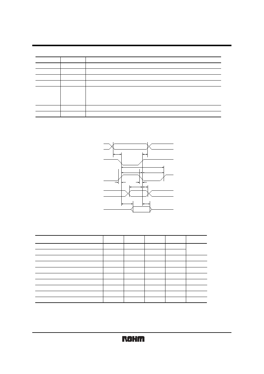
Timing chart
Writing
t
AW6
t
AH6
t
EWH
t
EWL
t
r
t
f
t
DS6
t
DH6
t
ACC6
t
OH6
RS
R / W
CSB
E
D0 to D7
(Write)
D0 to D7
(Read)
t
CYC6
Fig.6 interface (Write Operation)
Item
Terminal
Min.
Max.
Unit
Address hold time
Address set up time
System cycle time
Data setup time
Data hold time
Access time
Output disable time
"E" rise / fall time
"E" pulse width H level
"E" pulse width L level
In designing, please set the timing with sufficient margin
RS
RS
RS
D0 to D7
D0 to D7
D0 to D7
D0 to D7
E
E
E
Symbol
t
AH6
t
AW6
t
CYC6
t
DS6
t
DH6
t
ACC6
t
OH6
t
r
, t
f
t
EWH
t
EWL
ns
ns
ns
ns
ns
ns
ns
ns
ns
-
-
-
-
-
400
-
20
-
-
20
20
150
80
20
-
150
-
120
30
RCM2228R-A / B
Liquid Crystal Displays
5/7
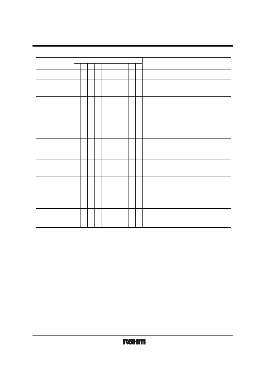
Instruction
Instruction
Display Clear
1.08ms
1.08ms
26.3
µ
s
26.3
µ
s
26.3
µ
s
26.3
µ
s
26.3
µ
s
26.3
µ
s
26.3
µ
s
26.3
µ
s
0
µ
s
0
RS
0
RW
0
D7
0
D6
0
D5
0
D4
0
D3
0
D2
0
D1
1
D0
Instruction Code
Description
Time
(MAX)
Cursor Home
0
0
0
0
0
0
0
0
1
Entry Mode Set
0
0
0
0
0
0
0
1
I / D S
Display ON / OFF
Control
0
0
0
0
0
0
1
D
C
B
Cursor or Display Shift
0
0
0
0
0
1
S / C R / L
Function Set
0
0
0
0
1
DL
N
CGRAM Address set
0
0
0
1
Busy flag
Address counter read
Data write
Data read
A5
A4
A3
A2
A1
A0
DDRAM Address set
0
0
1
A6 A5 A4 A3 A2 A1 A0
0
1
BF A6 A5 A4 A3 A2 A1 A0
1
0
D7 D6 D5 D4 D3 D2 D1 D0
1
1
D7 D6 D5 D4 D3 D2 D1 D0
Clears entire display and sets DDRAM
address 0 in address counter.
I / D : Specifies cursor / display shift
(I / D
=
1 :
+
1 I / D
=
0 :
-
1)
S : Executes the shift operation
(S
=
1: shift S
=
0 : no shift)
These operations are performed during data
write and read.
D: All display ON / OFF (1: ON , 0: OFF)
C: Cursor ON / OFF (1: ON , 0: OFF)
B: Cursor position blink
ON / OFF (1: ON , 0: OFF)
Shifts the cursor or display without changing
DDRAM data
S / C : (1: Display shift, 0: Cursor shift)
R / L : Specifies the shift direction
(1: Right shift 0: Left shift)
Sets function for the internal operation
DL : (1:8bit , 0:4bit)
N : (1:2line , 0:1line)
Assigns the CGRAM address
Assigns the DDRAM address
Writes data into DD / CGRAM
Read data from DD / CGRAM
BF: Reads the internal operation state
(1: In operation, 0: Completed operation)
AC: Reads the address counter value.
Sets DDRAM address 0 in the address
counter Shifted display returns to the
original state.
DDRAM data does not change.
Note: Refer to Instruction table for the list of each instruction execution time.
(
: don't care )