Äîêóìåíòàöèÿ è îïèñàíèÿ www.docs.chipfind.ru
RCM2234R-A / B
Liquid Crystal Displays
1/8
20 characters
×
2 lines COG module
RCM2234R-A / B
The RCM2234R-A / B is a reflective TN type liquid crystal module with a built-in controller / driver LSI and a display
capacity of 20 characters
×
2 lines.
Applications
Printers, Copiers, Facsimiles, etc
Features
(1) 5
×
7 dot character matrix with cursor.
(2) Interfaces with 4-bit, 8-bit MPUs.
(3) Displays up to 240 characters and special symbols.
(4) Custom character patterns are displayed with the character RAM.
(5) Abundant instruction set including clear display, cursor on/off, and character blinking.
(6) Compact and lightweight for easy assembly to the host instrument.
(7) Operable on single 5V power supply.
(8) Low power consumption.
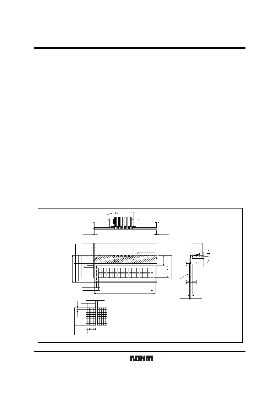
External dimensions (Unit : mm) (Viewing direction : 6 : 00)
24.9±0.3
No.1
No.15
81.0±0.3
0.3MAX.
1.0MAX.
2.0MAX.
(73.5)
79.0MIN.
10.0MAX.
(11.5)
12.5±0.3
26.3MIN.
(0.5)
10.15MIN.
13.15MIN.
23.15MAX.
26.15MAX.
(20.3)
28.3±0.3
8.0±0.3
2.7±0.3
±5
°
0.6
3.2
0.5
0.65
5.55
0.4
0.7±0.7
0.7±0.7
0.7±0.7
0.7±0.7
0.7±0.7
0.7±0.7
0.7±0.7
8.7±0.7
Over-coating resin
10.6±0.5
Dot detail
6.0MAX.
6.0MAX.
Viewing
direction
(6:00)
(PITCH1.8
×
14)25.2±0.3
±5
°
1.1±0.1
1.1±0.1
(0.3)
0.05
0.05
4.0MAX.
1.5MAX.
3.75±0.3
RCM2234R-A / B
Liquid Crystal Displays
2/8
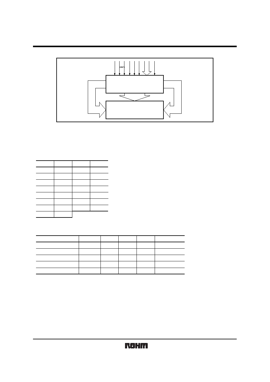
Block diagram
SEG1 to 100
20characters
×
2lines
COM
9 to 16
COM
1 to 8
E
R
S
R
/
W
V
S
S
V
L
C
D
I
V
D
D
D
B
0
t
o
D
B
7
G
N
D
V
R
Note 1. (V
LCDI
-V5)V is applied to LCD as driving voltage. Optimal driving voltage changes by viewing angle or temperature,
therefore adjusting V5 voltage in the condition that LCD is mounted on board is necessary.
2. Considering variation of power voltage and optimal driving voltage, V5 voltage should be adjustable.
3. V
R
: 10k
to 20k
(variable)
Fig.1
Pin assignments
Pin No.
1
2
3
4
5
symbol
Pin No.
symbol
V
SS
V
LCDI
9
DB2
V
DD
10
DB3
RS
11
DB4
R / W
12
DB5
13
DB6
6
E
14
DB7
7
DB0
15
GND
8
DB1
Absolute maximum ratings (Ta=25
°
C)
Parameter
Power voltage (1)
Power voltage (2)
Input voltage
Operation temperature
Storage temperature
Min.
-
0.3
-
0.3
-
0.3
0
Symbol
V
DD
V
LCDI
V
IN
Topr
Tstg
Max.
7.0
12.0
V
DD
+
0.3
50
70
Unit
V
V
V
°
C
°
C
Notes
-
-
Input terminal
-
-
-
20
Note 1.Use of LSI above the absolute maximum ratings may cause permanent LSI damage.
2.All voltage values are shown using V
SS
=0V as a reference.
3.Power supply must be retained in the relationship of V
DD
-V
SS
.
RCM2234R-A / B
Liquid Crystal Displays
3/8
Electrical characteristics (V
DD
=5.0V, Ta=25
°
C)
Parameter
Logic power voltage
LCD power voltage
H input voltage (1)
L input voltage (2)
H output voltage
L output voltage
LCD driving voltage
Symbol
V
DD
V
LCDI
V
IH
V
IL
V
OH
V
OL
fosc
V
LCD
Min.
4.75
3.0
0.7V
DD
V
SS
0.8V
DD
Typ.
5.0
-
Max.
5.25
5.0
V
DD
0.7
0.2V
DD
5.0
Unit
V
V
V
V
V
V
Conditions
IOH
= -
100
µ
A
IOL
=
100
µ
A
LCD drive resistance
-
-
-
-
-
-
-
325
kHz
250
175
3.0
Current consumption
I
DD
700
1400
µ
A
Check pattern
-
Clock oscillation frequency
Terminal Name
E, RS, SEL1,
DB0 to DB7
DB0 to DB7
V
DD
Optical characteristics (Ta=25
°
C)
(1) Viewing direction 6:00
Parameter
Response time
Response time
Contrast ratio
Viewing angle
Symbol
t
r
t
d
K
1
2
Min.
-
-
-
-
20
±
30
Typ.
100
150
3
-
-
-
Max.
250
250
-
0
-
-
Unit
ms
ms
-
deg
deg
Test Conditions
=
10
°
,
=
0
°
K 1.2
=
0
°
K 1.2
=
20
°
=
10
°
,
=
0
°
=
10
°
,
=
0
°
(2) Viewing direction 12:00
Parameter
Symbol
t
r
t
d
K
1
'
2
'
Min.
-
-
-
-
20
150 to 210
Typ.
100
150
3
-
-
-
Max.
250
250
-
0
-
-
Unit
ms
ms
-
deg
deg
Test Conditions
'
=
10
°
,
=
180
°
K 1.2
=
180
°
K 1.2
'
=
20
°
'
=
10
°
,
=
180
°
'
=
10
°
,
=
180
°
Response time
Response time
Contrast ratio
Viewing angle
RCM2234R-A / B
Liquid Crystal Displays
4/8
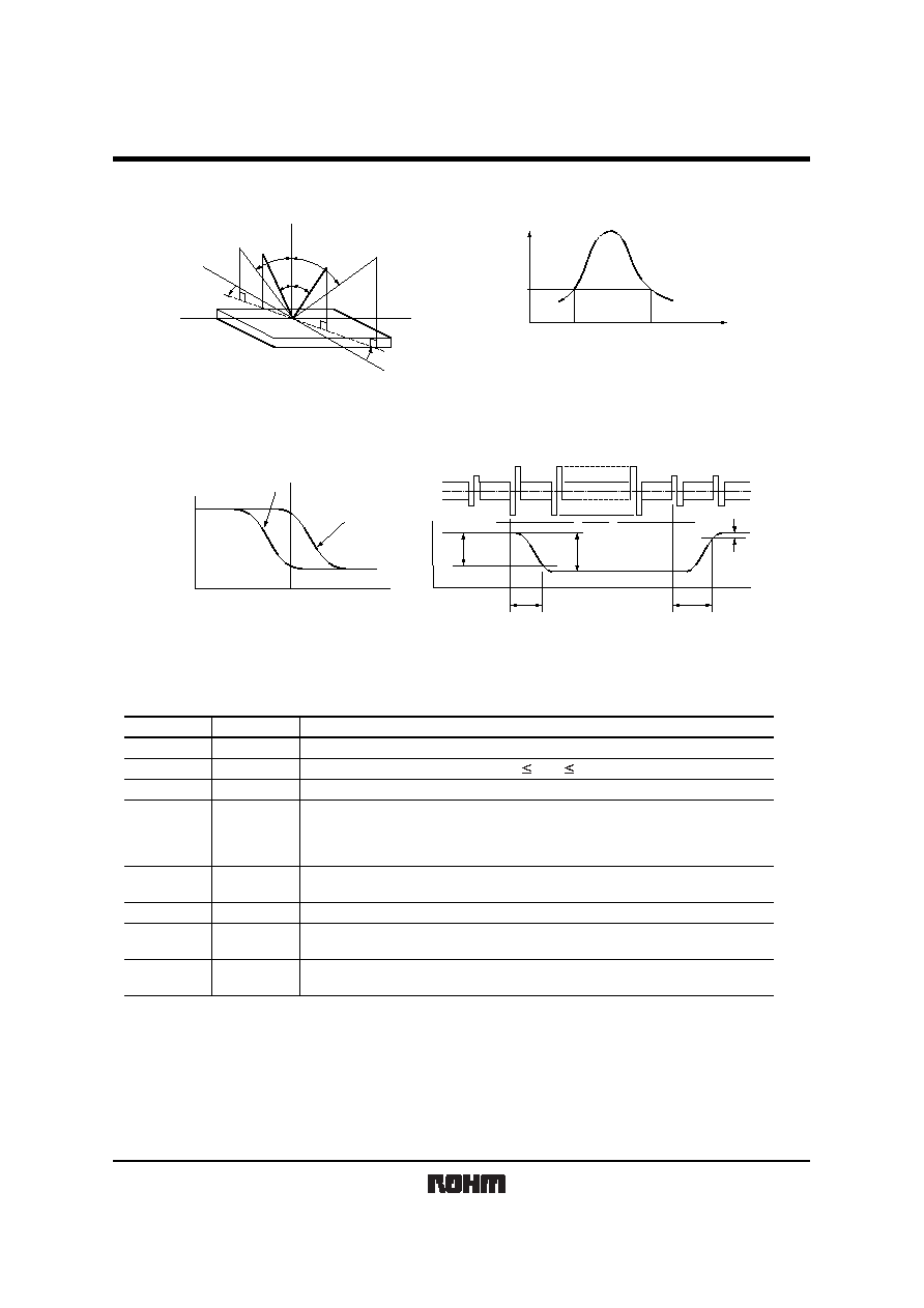
90%
100%
10%
t
r
t
d
100
0
B
1
B
2
K=B
2
/ B
1
1.2
1
2
Viewing direction
12 o'clock
Viewing direction 6 o'clock
X
X'
2
2'
1
1'
Y (
=
180
°
)
Y' (
=180
°
)
Z (
=0
°
)
Fig.2
Fig.4
Fig.3
Fig.5
Selected condition
Rise time
Fall time
Non-selected
Selected
Brightness (%)
Driving voltage
Viewing angle
Contrast ratio
(1) Definition
and
(3) Definition of contrast ratio "K"
(2) Definition of viewing angles
1 and
2
(4) Definition of optical response
Terminal function
V
SS
V
LCDI
RS
R / W
E
V
DD
Symbol
Input
Input
DB0 to DB3
Input / Output
Input
Input
Input
Input / Output
Input
I/O Terminal
Function
V
SS
=
0V
LCD driving voltage input terminal 3.0 V
LCDI
5.0
V
DD
=
4.75 to 5.25V
Register selected signal
L: Instruction register (at write)
Busy flag / address counter (at read)
H: Data register (at write & read)
Read / Write select signal
L: Write H: Read
Data Read / Write enable signal
Data bus four-state bi-directional
Data bus four-state bi-directional
DB4 to DB7
RCM2234R-A / B
Liquid Crystal Displays
5/8
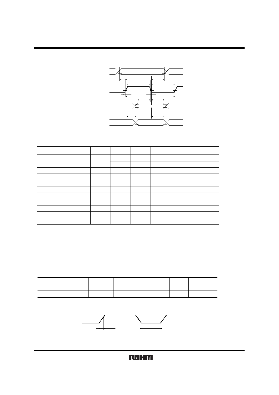
Timing characteristics
Write operation
t
AS
t
AH
t
WH
t
WL
t
r
t
f
v
OL
v
OH
v
OL
v
OH
v
IL
v
IH
v
IL
v
IH
v
IL
v
IH
v
IL
v
IH
v
IL
v
IH
v
IL
v
IH
t
ACC
t
CH
RS
R / W
E
D0 to D7
D0 to D7
Fig.6
read data
write data
t
DS
t
CYC
t
DH
Item
Min.
Typ.
Max.
Unit
Address set up time
Address hold time
"E" pulse width H level
"E" pulse width L level
Cycle time
Data setup time
Data hold time
Output disable time
Output data hold time
"E" rise / fall time
Symbol
t
AS
t
AH
t
WH
t
WL
t
CYC
t
DS
t
DH
t
ACC
t
CH
t
r
, t
f
ns
ns
ns
ns
ns
ns
ns
ns
ns
ns
ns
Condition
at write
at read
95
10
120
120
20
500
500
1000
200
20
40
Numbers above mentioned are driver IC's number as a single unit.
In designing, please set the timing with sufficient margin.
Reset Circuit
Item
Power rise time
Power OFF time
Symbol
t
rDD
t
OFF
Min.
0.1
1
Typ.
-
-
Max.
10
-
Unit
ms
ms
Condition
-
-
The busy flag indicating internal operating state is H level in the period of 2ms after Reset operation starting.
External input is not available in this state. After 2ms passes or confirms the busy flag is L level the instruction
can be acceptable.
If the power supply conditions are not met, the integrated reset circuit will not operate properly. Execute
initialization by instruction.
Note : The power OFF time specifies the time during which the power is off when the instantaneous power failure occurs or power ON/OFF repeated.
t
rDD
t
OFF
0.2V
0.9V
DD
0.2V
0.2V
V
DD
Document Outline