 | –≠–ª–µ–∫—Ç—Ä–æ–Ω–Ω—ã–π –∫–æ–º–ø–æ–Ω–µ–Ω—Ç: RPM871 | –°–∫–∞—á–∞—Ç—å:  PDF PDF  ZIP ZIP |

RPM871-H7
Photo Link Module
IrDA Infrared communication Module
RPM871-H7
RPM871-H7 is an infrared communication module for IrDA Ver. 1.2 (Low Power). The infrared LED, PIN photo diode,
waveform shaping LSI are all integrated into a single package. This module is designed with power down function and
low current consumption at stand-by mode. The ultra small package makes it a perfect fit for mobile devices.
!
!
!
!
Features
1) Applied to IrDA version 1.2. (Low Power)
2) Designed for low power consumption at stand-by for receiving (Typ.73
µA).
3) Suitable for sets driven by battery due to power down control function.
4) Power supply voltage range : 2.6V
3.6V
5) Constant LED load resistance can change communication range. (Approx. 20
60cm)
!
!
!
!
Applications
Cellular phones, PDAs, etc.
!
!
!
!
Absolute maximum ratings (Ta = 25
∞C)
Parameter
Symbol
Limits
Unit
Power supply voltage
V
CC
-
0.3~
+
7.0
-
20~
+
85
-
30~
+
100
V
mA
mW
200
2
150
1
Operating temperature range
Storage temperature range
LED peak current
Power dissipation
Topr
Tstg
I
FP
Pd
∞
C
∞
C
1 70mm
◊
70mm, t=1.6mm, glass epoxy mounting. Derating : 2mW/
∞
C for operation above Ta=25
∞
C
2 LED peak current
<
90
µ
s. ON duty
<
20%
!
!
!
!
Recommended operating conditions (Ta = 25
∞C)
Parameter
Symbol
Min.
Typ.
Max.
Unit
Power supply voltage
V
CC
2.8
V
2.6
3.6
V
LEDA
2.8
V
2.6
5.5
RPM871-H7
Photo Link Module
!
!
!
!
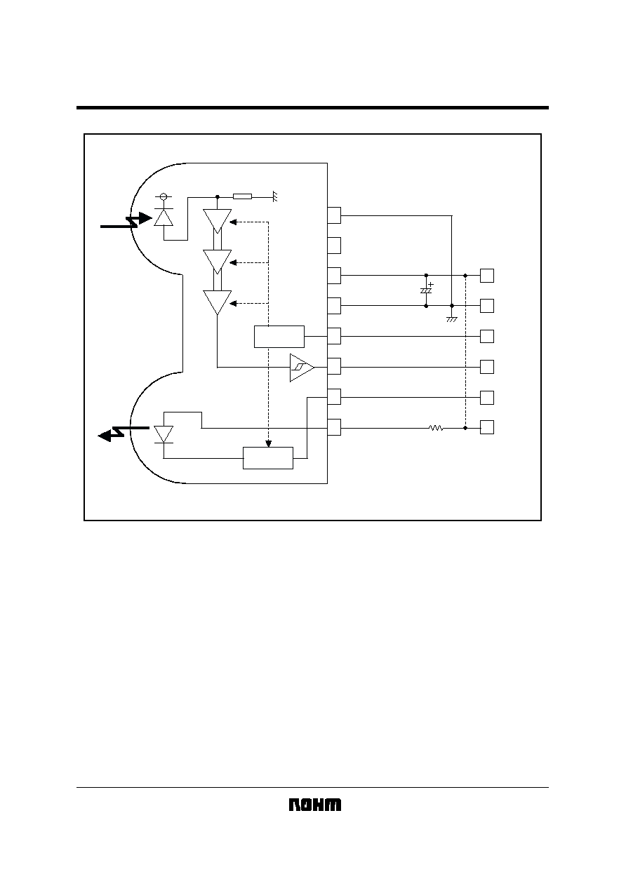
Block diagram and application circuit
AMP
1
8
76543
2
AMP
AMP
POWER
DOWN
LED
DRIVER
V
CC
V
CC
GND
C1
R1
GND
NC
GND
PWDOWN
RXD
TXD
LEDA
PWDOWN
RXD
TXD
(LEDV
CC
)
V
CC
(3pin) and VLEDA (8pin) can be used on
either common power source or different one.

RPM871-H7
Photo Link Module
!
!
!
!
Terminal description
Terminal
Circuit
Function
Pin No
1, 4
GND
GND
Pin1 and pin4 must be connected to the
ground.
This Terminal must be left open.
Connect to Ground.
Power-down Control Terminal
CMOS Logic Level Input
When input is H, it will stop the receiving
circuit, Pin-PD current and transmitting
LED operation.
H : POWERDOWN
L : OPERATION
Receiving Data Output Terminal
CMOS Logic Level Output
When PWDOWN (5pin)=H, the RXD
output will be pulled up to V
CC
at
approximately 300k
.
Transmitting Data Input Terminal
H : LED (PWDOWN=L)
CMOS Logic Level Input
Holding TXD="H" status, LED will be
turn off approximately 45
µ
s.
LED ANODE Terminal
Other power source can be used
difference between LEDV
CC
and V
CC
.
LED current depends on LED load
resistance value.
2
NC
PWDOWN
RXD
TXD
LEDA
Shield Case
3
5
6
7
8
-
V
CC
V
CC
For preventing from infection, connect
a capacitor between V
CC
(3pin) and
GND (4pin).
V
CC
V
CC
200K
LED
V
CC
V
CC
300k
PWDOWN
RPM871-H7
Photo Link Module
!
!
!
!
Electrical characteristics (Unless otherwise noted, V
CC
=2.8V, VLEDV
CC
=2.8V, Ta = 25
∞C)
Parameter
Symbol
Min.
Typ.
Max.
Unit
Conditions
Consumption current1
I
CC
1
I
CC
2
VPDH
VPDL
IPDH
IPDL
73
µ
A
Stand-by for receiving At no input light
PWDOWN PIN High At no input light
PWDOWN
=
V
CC
[V]
Consumption current2
Transmission rate
PWDOWN INPUT High voltage
PWDOWN INPUT Low voltage
PWDOWN INPUT High current
PWDOWN INPUT Low current
TXD INPUT High voltage
TXD INPUT Low voltage
RXD OUTPUT High voltage
RXD OUTPUT rise time
RXD OUTPUT fall time
RXD OUTPUT pulse width
Receiver latency time
RXD OUTPUT Low voltage
TXD INPUT High current
TXD INPUT Low current
LED ANODE current
-
0.01
-
-
-
2.4
-
-
V
CC
-
0.55
99
µ
A
0.2
kbps
115.2
V
V
-
0.55
<Transmitter>
<Receiver>
VTXH
VTXL
ITXH
ITXL
ILEDA
VRXH
VRXL
tRR
tFR
tRT
twRXD
PWDOWN
=
0 [V]
TXD
=
V
CC
[V]
TXD
=
0 [V]
R1
=
7.5 [
]
0
-
1.0
V
CC
-
0.55
-
7
-
1.0
-
-
-
-
1.5
-
V
CC
-
0.5
0
-
1.0
-
-
14
0
144
-
-
70
30
2.3
100
µ
A
1.0
µ
A
1.0
V
V
µ
A
µ
A
mA
V
V
ns
ns
µ
s
µ
s
-
0.55
28
1.0
-
-
0.4
-
-
3.6
300
IRXH
=-
50
µ
A
IRXL
=
200
µ
A
C
L
=
15pF
C
L
=
15pF
C
L
=
15pF, 2.4
115.2kbps
!
!
!
!
Optical characteristics (Unless otherwise noted, V
CC
=2.8V, VLEDV
CC
=2.8V, Ta = 25
∞C)
Parameter
Symbol
Min.
Typ.
Max.
Unit
Conditions
Peak wave length
1. This product is not designed for protection against radioactive rays.
2. This product dose not include laser transmitter.
3. This product includes one PIN photo diode.
4. This product dose not include optical load.
P
IE1
L/2
D/2
TLEDmax
Tr/Tf
Tj
Ee
870
nm
-
15
∞
L
15
∞
R1
=
7.5 [
]
-
15
∞
L
15
∞
TXD
=
V
CC
10%
90%
Intensity1
Half-angle
Rise time / Fall time
Optical over shoot
Edge jitter
Irradiance in angular
INPUT Half-Angular
Maximum emitting time
850
36
14.4
-
±
18
-
-
900
mW/Sr
93.6
mW/cm
2
deg
ns
deg
µ
s
±
30
100
-
-
-
-
-
45
-
40
0.0068
±
15
10
%
25
ns
40
500
-
96
RPM871-H7
Photo Link Module
!
!
!
!
Timing chart
less than 45
µ
s
(emitting)
more than 45
µ
s
approximately 45
µ
s
less than 2.3
µ
s
more than 2.3
µ
s
approximately 2.3
µ
s
approximately 2.3
µ
s
pull up to V
CC
at approximately 300k
(emitting)
(emitting)
(Emitting side)
(Detecting side)
TXD
(7pin)
Internal LED
(Light output)
Light input
RXD
(6pin)
PWDOWN
(5pin)
!
!
!
!
Attached components
Recommended values
Part symbol
C1
Recommended value
Notice
1
µ
F, tantalum or ceramic
Ex.) TCFGA1A105M8R (ROHM)
Bigger capacitance is recommended with much noise from power supply
R1
7.5
±
5%, 1/4W
(VLEDV
CC
=
2.8V)
More than 60cm distance, more than 4[
µ
W/cm
2
] at detecting side.
(vs ver1.0)
More than 46cm distance, more than 6.8[
µ
W/cm
2
] at detecting side.
(vs RPM871-H7)
In case of using R1 with different condition from the above, formula is as follows :
LED resistance value : R1[
], LED average consumption current : ILED[mA], Supply voltage : VLEDV
CC
[V],
Link distance : d[cm] (Including LED's distribution within
±15deg)
R1=T
◊ (VLEDV
CC
-1.45) / d
2
-3.5 []
ILED=Duty
◊ (VLEDVCC-1.36) / (R1+2.5) [A]
Duty : LED duty at emitting
T : 17300 (vs. RPM871-H7), 29400 (vs. ver1.0)
Please set up to be ILED / Duty < 200[mA] (Duty < 20%)