EMB3 / UMB3N / IMB3A
Transistors
General purpose (dual digital transistors)
EMB3 / UMB3N / IMB3A
!
!
!
!
Features
1) Two DTA143T chips in a EMT or UMT or SMT
package.
2) Mounting possible with EMT3 or UMT3 or SMT3
automatic mounting machines.
3)
Transistor elements are independent, eliminating
interference.
!
!
!
!
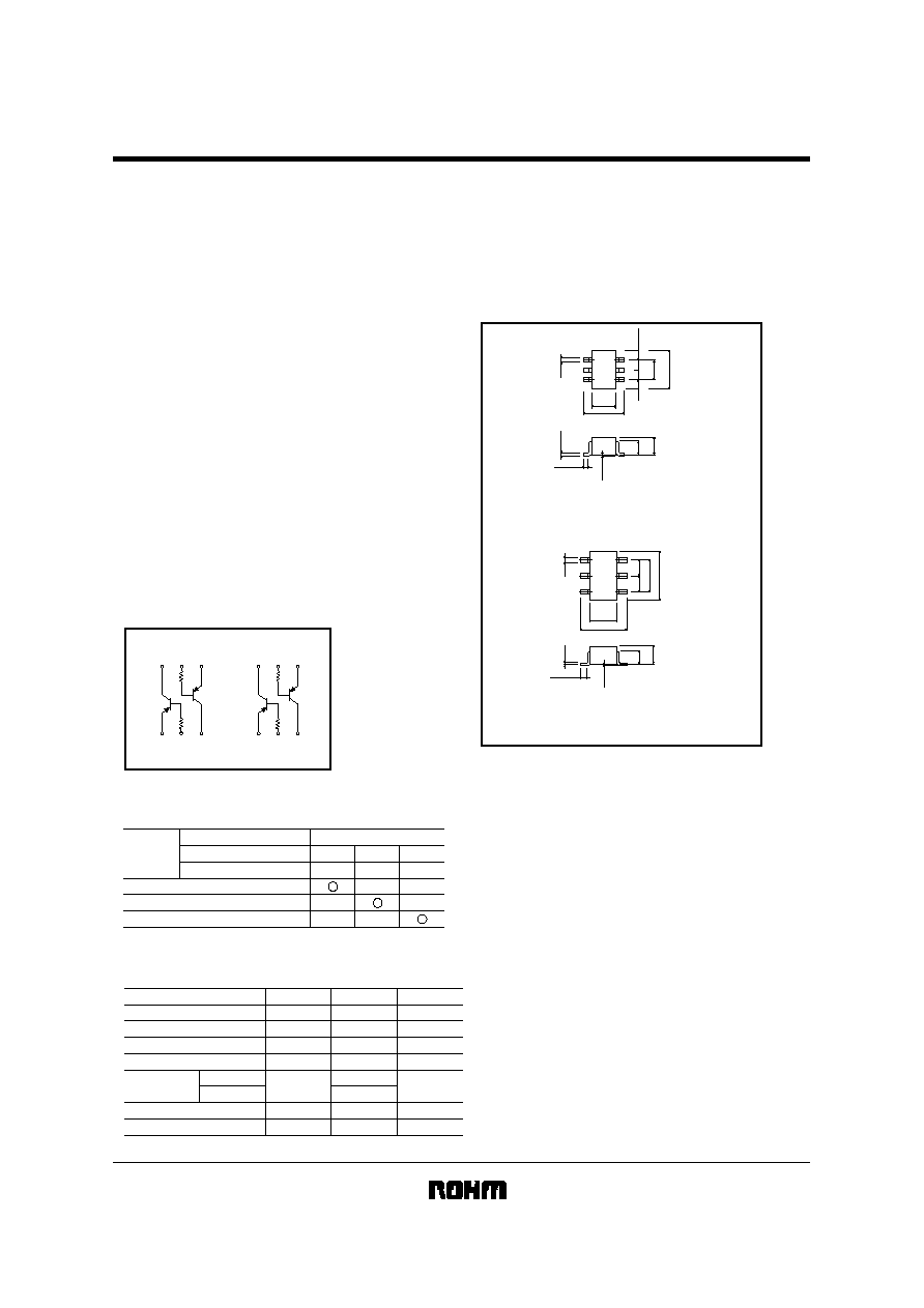
Structure
Dual PNP digital transistor
(each with single built in resistor)
The following characteristics apply to both DTr
1
and DTr
2
.
!
!
!
!
Equivalent circuit
DTr
2
DTr
1
(3)
(2)
(1)
(3)
(2)
(1)
(4)
(5)
(6)
(4)
(5)
(6)
R
1
R
1
DTr
2
DTr
1
R
1
R
1
R
1
=4.7k
R
1
=4.7k
EMB3, UMB3N
IMB3A
!
!
!
!
Packaging specifications
Package
Taping
Code
UMB3N
EMB3
Type
IMB3N
TN
3000
-
-
T2R
8000
-
-
T110
3000
-
-
Basic ordering unit (pieces)
!
!
!
!
External dimensions (Units : mm)
ROHM : UMT6
EIAJ : SC-88
ROHM : SMT6
EIAJ : SC-74
EMB3, UMB3N
IMB3A
Abbreviated symbol: B3
Abbreviated symbol: B3
Each lead has same dimensions
0to0.1
( 6
)
2.0
1.3
0.9
0.15
0.7
0.1Min.
2.1
0.65
0.2
1.25
( 1
)
0.65
( 4
)
( 3
)
( 2
)
( 5
)
Each lead has same dimensions
( 6
)
( 5
)
( 4
)
0.3to0.6
0.15
0.3
1.1
0.8
0to0.1
( 3
)
2.8
1.6
1.9
2.9
0.95
( 2
)
0.95
( 1
)
!
!
!
!
Absolute maximum ratings (Ta = 25
∞C)
Parameter
Symbol
Limits
Unit
V
CBO
-
50
V
V
CEO
-
50
V
V
EBO
-
5
V
I
C
-
100
mA
Tj
150
∞
C
Tstg
-
55~
+
150
∞
C
P
C
EMB3,UMB3N
150 (TOTAL)
mW
IMB3A
300 (TOTAL)
1
2
Collector-base voltage
Collector-emitter voltage
Emitter-base voltage
Collector current
Junction temperature
Storage temperature
Collector power
dissipation
1 120mW per element must not be exceeded.
2 200mW per element must not be exceeded.
EMB3 / UMB3N / IMB3A
Transistors
!
!
!
!
Electrical characteristics (Ta = 25
∞C)
Parameter
Symbol
BV
CBO
BV
CEO
BV
EBO
I
CBO
I
EBO
h
FE
V
CE (sat)
R
1
Min.
-
50
-
50
-
5
-
-
100
-
3.29
-
-
-
-
-
250
-
4.7
-
-
-
-
0.5
-
0.5
600
-
0.3
6.11
V
I
C
=
-
50
µ
A
I
C
=
-
1mA
I
E
=
-
50
µ
A
V
CB
=
-
50V
V
EB
=
-
4V
V
CE
=
-
5V, I
C
=
-
1mA
-
I
C
/I
B
=
-
5mA/
-
2.5mA
V
V
µ
A
µ
A
-
V
k
Typ.
Max.
Unit
Conditions
f
T
-
250
-
V
CE
=10mA, I
E
=
-
5mA, f=100MHz
MHz
Collector-base breakdown voltage
Collector-emitter breakdown voltage
Emitter-base breakdown voltage
Collector cutoff current
Emitter cutoff current
DC current transfer ratio
Transition frequency
Collector-emitter saturation voltage
Input resistance
Transition frequency of the device
!
!
!
!
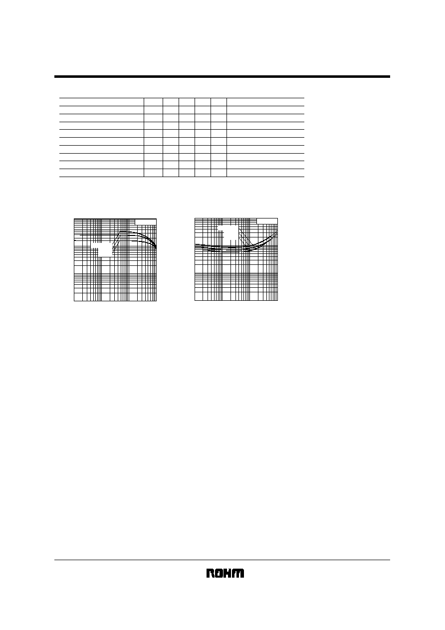
Electrical characteristic curves
V
CE
=
-
5V
-
100
µ
-
1m
-
10m
-
200
µ
-
2m
-
20m
-
500
µ
-
5m
-
50m
-
100m
1k
500
200
100
50
20
10
5
2
1
DC CURRENT GAIN : h
FE
COLLECTOR CURRENT : I
C
(A)
Fig.1 DC current gain vs. collector
current
-
40
∞
C
25
∞
C
Ta=100
∞
C
l
C
/l
B
=20
-
500m
-
200m
-
100m
-
50m
-
20m
-
10m
-
5m
-
2m
-
1m
-
1
-
100
µ
-
1m
-
10m
-
200
µ
-
2m
-
20m
-
500
µ
-
5m
-
50m
-
100m
COLLECTOR SATURATION VOLTAGE : V
CE(sat)
(V)
COLLECTOR CURRENT : I
C
(A)
Fig.2 Collector-emitter saturation
voltage vs. collector current
Ta=100
∞
C
25
∞
C
-
40
∞
C