EMH2 / UMH2N / IMH2A
Transistors
General purpose (dual digital transistors)
EMH2 / UMH2N / IMH2A
!
!
!
!
Features
1) Two DTC144Es chips in a EMT or UMT or SMT
package.
2) Mounting possible with EMT3 or UMT3 or SMT3
automatic mounting machines.
3) Transistor elements are independent, eliminating
interference.
4) Mounting cost and area can be cut in half.
!
!
!
!
Structure
Epitaxial planar type
NPN silicon transistor
(Built-in resistor type)
The following characteristics apply to both DTr
1
and DTr
2
.
!
!
!
!
Equivalent circuit
R
1
=47k
R
2
=47k
R
1
=47k
R
2
=47k
DTr
2
DTr
1
(3)
(2)
(1)
(4)
(5)
(6)
R
1
R
2
R
2
R
1
DTr
2
DTr
1
(4)
(5)
(6)
(3)
(2)
(1)
R
1
R
2
R
2
R
1
EMH2 / UMH2N
IMH2A
!
!
!
!
Packaging specifications
Package
Code
T2R
T110
8000
3000
-
-
-
-
-
-
TN
3000
Taping
Basic ordering
unit (pieces)
UMH2N
EMH2
IMH2A
Type
!
!
!
!
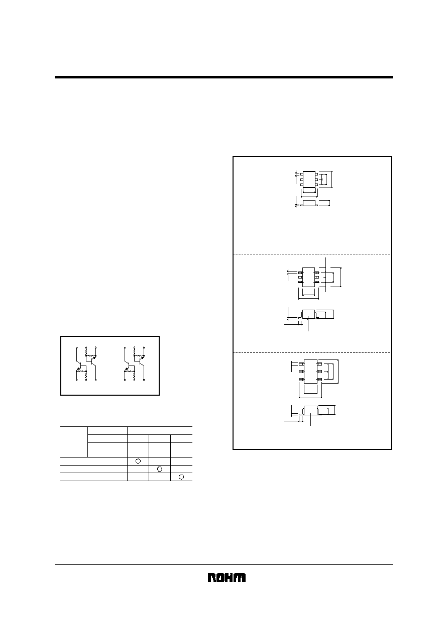
External dimensions (Units : mm)
ROHM : EMT6
ROHM : SMT6
EIAJ : SC-74
EMH2
IMH2A
ROHM : UMT6
EIAJ : SC-88
UMH2N
Abbreviated symbol : H2
Abbreviated symbol : H2
Abbreviated symbol : H2
All terminals have same dimensions
All terminals have same dimensions
All terminals have same dimensions
0.22
1.2
1.6
(1)
(2)
(5)
(3)
(6)
(4)
0.13
0.5
0.5
0.5
1.0
1.6
0to0.1
( 6
)
2.0
1.3
0.9
0.15
0.7
0.1Min.
2.1
0.65
0.2
1.25
( 1
)
0.65
( 4
)
( 3
)
( 2
)
( 5
)
( 6
)
( 5
)
( 4
)
0.3to0.6
0.15
0.3
1.1
0.8
0to0.1
( 3
)
2.8
1.6
1.9
2.9
0.95
( 2
)
0.95
( 1
)

EMH2 / UMH2N / IMH2A
Transistors
!
!
!
!
Absolute maximum ratings (Ta = 25
∞C)
Parameter
Symbol
Limits
Unit
V
CC
50
V
V
IN
-
10
40
V
I
O
30
mA
I
C(Max.)
100
Tstg
-
55~
+
150
∞
C
Pd
EMH2,UMH2N
150 (TOTAL)
mW
IMH2A
300 (TOTAL)
Tj
150
∞
C
1
2
Supply voltage
Input voltage
Output current
Junction temperature
Storage temperature
Power
dissipation
1 120mW per element must not be exceeded.
2 200mW per element must not be exceeded.
!
!
!
!
Electrical characteristics (Ta = 25
∞C)
Parameter
Symbol
V
I(off)
V
I(on)
V
O(on)
I
I
G
I
R
1
Min.
-
3
-
-
68
32.9
-
-
0.1
-
-
47
0.5
-
0.3
0.18
-
61.1
V
V
CC
=5V, I
O
=100
µ
A
V
O
=0.3V, I
O
=2mA
I
O
/I
I
=10mA/0.5mA
V
I
=5V
V
O
=5V, I
O
=5mA
-
V
mA
I
O(off)
-
-
0.5
V
CC
=50V, V
I
=0V
µ
A
-
k
R
2
/R
1
0.8
1
1.2
-
-
Typ.
Max.
Unit
Conditions
-
f
T
250
-
V
CE
=10mA, I
E
=
-
5mA, f=100MHz
MH
Z
Input voltage
Output voltage
Input current
DC current gain
Transition frequency
Input resistance
Output current
Resistance ratio
Transition frequency of the device
!
!
!
!
Electrical characteristic curves
V
O
=0.3V
100
µ
200
µ
500
µ
1m
2m
5m 10m 20m
50m100m
100
50
20
10
5
2
1
500m
200m
100m
INPUT VOLTAGE : V
I(on)
(V)
OUTPUT CURRENT : I
O
(A)
25
∞
C
100
∞
C
Ta=
-
40
∞
C
Fig.1 Input voltage vs. output current
(ON characteristics)
V
CC
=5V
0.5
1.0
1.5
2.0
2.5
3.0
0
10m
5m
2m
1m
500
µ
200
µ
100
µ
50
µ
20
µ
10
µ
5
µ
1
µ
2
µ
INPUT VOLTAGE : V
I (off)
(V)
OUTPUT CURRENT : Io
(A)
Ta=100
∞
C
25
∞
C
-
40
∞
C
Fig.2 Output current vs. input voltage
(OFF characteristics)
OUTPUT CURRENT : I
O
(A)
DC CURRENT GAIN : G
I
V
O
=5V
100
µ
200
µ
500
µ
1m
2m
5m 10m 20m 50m100m
1k
500
200
100
50
20
10
5
2
1
Fig.3 DC current gain vs. output
current
Ta=100
∞
C
25
∞
C
-
40
∞
C
