This Data Sheet states Saifun's current technical specifications regarding the Products described herein. This Data Sheet
may be revised by subsequent versions or modifications due to changes in technical specifications.
Publication# 1910 Rev: 1.1 Amendment: 1
Issue Date: January 27, 2003
SA25C1024
Data Sheet
Features
∑=
Saifun NROMTM Flash Cell
∑=
Serial Peripheral Interface (SPI) Compatible
∑=
Supports SPI Modes 0 (0,0) and 3 (1,1)
∑=
Byte and Page Write Modes (up to 128 bytes)
∑=
Single Supply Voltage:
≠
2.7V to 3.6V (L)
≠
4.5V to 5.5V (H)
∑=
10MHz Clock Rate
∑=
Block Write Protection:
≠
Protect º, Ω, or Entire Array
∑=
Write Protect Pin and Write Disable Instructions of both Hardware and
Software Data Protection
∑=
Self-timed Write Cycle (10mS max)
∑=
100,000 Write Cycles (Minimum)
∑=
20 Year Data Retention
∑=
Low-power Standby Current (less than 1
µ
µ
µ
µA)
∑=
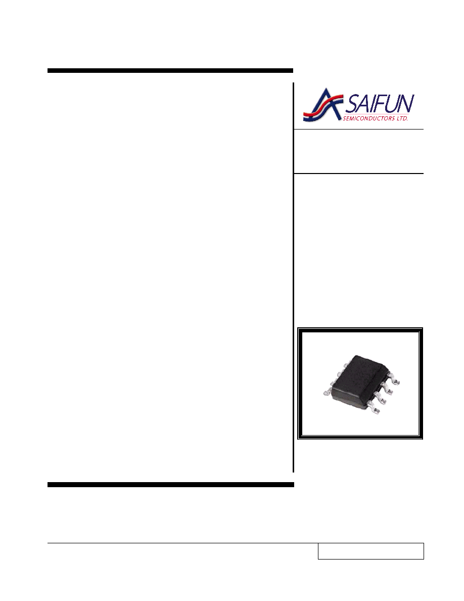
8-SOIC Narrow Package (0.150" Wide Body, JEDEC SOIC)
∑=
Temperature Range:
≠
Industrial: -40∞C to +85∞C
≠
Commercial: 0∞C to +70∞C
General Description
SA25C1024 is a 1Mb CMOS non-volatile serial EEPROM,
organized as a 128K x 8-bit memory. The SA25C1024 is
available in a space-saving, 8-lead narrow SOIC package. In
addition, it is available in a wide range of voltages ≠ 2.7-3.6 V
and 4.5-5.5 V.
The SA25C1024 is enabled through the Chip Select (CSb) pin
and is accessed via a 3-wire interface consisting of Serial Data
Input (SI), Serial Data Output (SO) and Serial Data Clock
(SCK). All write cycles are completely self-timed, and no
separate ERASE cycle is required before write.
(continued)
1Mb EEPROM SPI
with 10MHz and Low
Standby
http://www.saifun.com
Saifun NROM
TM
is a trademark of Saifun Semiconductors Ltd.

SA25C1024 Data Sheet
SAIFUN
2
Table of Contents
Features ......................................................................... 1
General Description ...................................................... 1
Ordering Information .................................................... 5
Product Specifications ................................................. 6
Absolute Maximum Ratings..................................... 6
Latch Up Specifications........................................... 6
ESD Specifications.................................................. 6
Operating Conditions............................................... 6
DC Characteristics ........................................................ 7
AC Test Conditions ....................................................... 8
Serial Interface Description .......................................... 9
Master ..................................................................... 9
Slave ....................................................................... 9
Transmitter/Receiver ............................................... 9
Serial Opcode ......................................................... 9
Invalid Opcode ........................................................ 9
Chip Select (CSb).................................................... 9
HOLDb .................................................................... 9
Write Protect ........................................................... 9
Functional Description ............................................... 10
Write Enable (WREN) ........................................... 10
Write Disable (WRDI)............................................ 10
Read Status Register (RDSR) ............................... 11
Write Status Register (WRSR) .............................. 11
Read Sequence (READ) ....................................... 11
Write Sequence (WRITE)...................................... 12
Timing Diagrams ......................................................... 13
Physical Dimensions .................................................. 16
Life Support Policy...................................................... 19
List of Figures
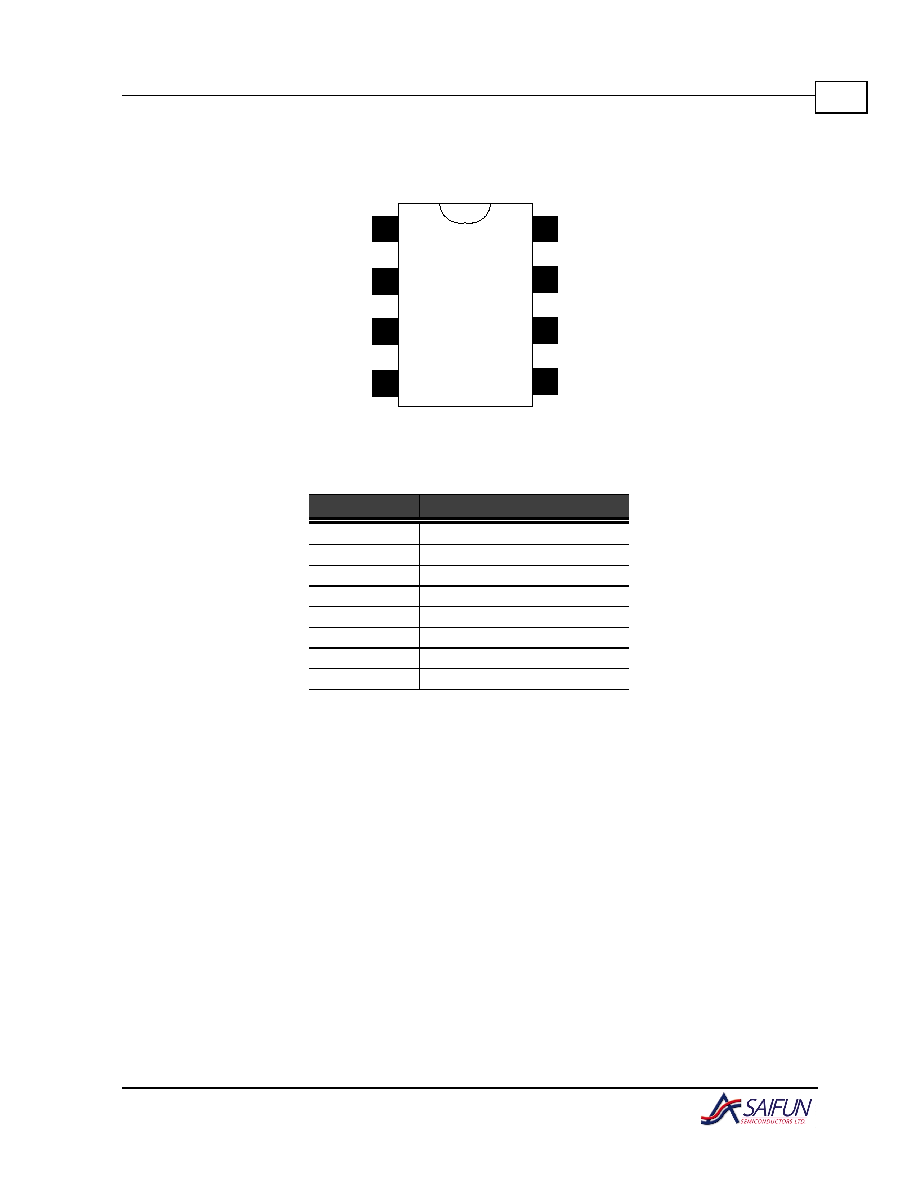
Figure 1. SOIC 8 ≠ Narrow/PDIP Package (Top View) .... 4
Figure 2: SA25C1024 Ordering Information..................... 5
Figure 3. AC Measurements I/O Waveform..................... 8
Figure 4. SPI Serial Interface ........................................ 10
Figure 5. SPI Mode 0 (0,0) Timing................................. 13
Figure 6. SPI Mode 0 (0,0) and 3 (1,1) Timing............... 13
Figure 7. HOLDb Timing ............................................... 14
Figure 8. Read Timing................................................... 14
Figure 9. Write Timing................................................... 14
Figure 10. Write Status Register Timing........................ 15
Figure 11. Read Status Register Timing........................ 15
Figure 12. 8-pin SOIC Package..................................... 16
Figure 13. 8-pin Molded Small Outline Package (MN),
0.150" Wide Body, JEDEC SOIC......................... 17
Figure 14. Molded Dual-in-line Package (N) Package
Number N08E...................................................... 18
List of Tables
Table 1. Pin Names......................................................... 4
Table 2. DC Characteristics............................................. 7
Table 3. AC Measurements............................................. 8
Table 4. AC Characteristics............................................. 8
Table 5. Instruction Set ................................................. 10
Table 6. Status Register Format.................................... 10
Table 7. Block Write Protect Bits................................... 11
Table 8. WPBEN Operation .......................................... 11
Table 9. Read Status Register Definition....................... 12