
sames
sames
sames
sames
sames
FEATURES
!
Performs bidirectional energy meter-
ing and includes a 7 digit LCD driver
with announciators
!
4 externally selectable on-chip tariff
registers
!
An additional total energy register
!
Meets the accuracy requirements for
Class 1 AC Watt hour meters
!
Optical interface for electronic reading
according to IEC1107 Mode D
1/12
!
Pulse output for calibration
!
Total power consumption rating below
600mW
!
Uses a shunt resistor for current sens-
ing
!
Operates over a wide temperature
range
!
Demonstration software included
MONOCHIP SINGLE PHASE BIDIRECTIONAL
KILOWATT HOUR METERING MODULE
PM9109BFX
PDS038-SA9109-001
REV. 3
28-06-00
SA9109B APPLICATION NOTE
PM9109BF
DESCRIPTION
The SAMES monochip single phase bidirectional kilowatt hour metering module, the
PM9109BF, provides all the required metering functions including energy measure-
ment, a 7 digit LCD driver, a tariff selection facility, an optical port as well as a pulse
output for calibration purposes.
Energy consumption is determined by the power measurement being integrated over
time.
This method of calculation takes the power factor into account.
This application utilises the SAMES SA9109BFA monochip single phase bidirectional
kilowatt hour metering IC for energy measurement.
As a safety measure, this application shows the current sensor connected to the neutral
line. In practice the live line may be used for current sensing, provided that the supply
connections (MAINS) are reversed on the module.
PM9109BF
2/18
sames
sames
sames
sames
sames
ABSOLUTE MAXIMUM RATINGS*
Parameter
Symbol
Min
Max
Unit
Supply Voltage (Note 1)
V
AC
540
V
Current Sense Input (Note 1)
V
IV
-2.5
V
Storage Temperature
T
STG
-25
+125
�C
Operating Temperature
T
O
-10
+70 (Note 2)
�C
Max Current
I
MAX
800 (Note 3)
A
through sensor
I
MAX
2000 (Note 4)
A
Note 1:
Voltages are specified with reference to Live.
Note 2:
The SA9109B integrated circuit is specified to operate over the temperature
range -10�C to +70�C. The module functionality will however depend upon
the external components used.
Note 3:
t = 500ms
Note 4:
t = 1ms
*Stresses above those listed under "Absolute Maximum Ratings" may cause permanent
damage to the device. This is a stress rating only. Functional operation of the device
at these or any other conditions above those indicated in the operational sections of
this specification, is not implied. Exposure to Absolute Maximum Ratings for extended
periods may affect device reliability.
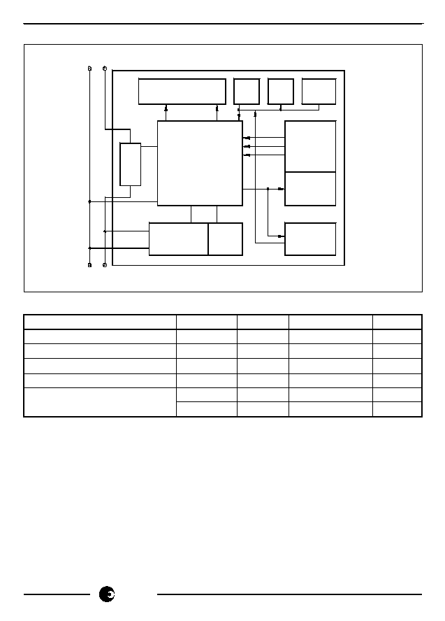
BLOCK DIAGRAM
SCROLL
SA9109B
N
L
SHUNT
PO W ER
SUP PL Y
BAT T ERY
BAC KUP
LOAD
DIS PLAY
DR-00995
OPTICAL
PORT
PULSE
OUTPUT
ISOLATED
CALIBRATION
INTERFACE
PGM
DTA
CLK
RES ET
T AR IF F
SEL ECT

PM9109BF
sames
sames
sames
sames
sames
3/18
ELECTRICAL CHARACTERISTICS
(Over the temperature range -10�C to +70�C, unless otherwise specified. Power
consumption figures are applicable to the PM9109BFE only.)
Parameter
Symbol
Min
Typ
Max
Unit
Condition
Supply Voltage
V
AC
180
230
265
V
PM9109BFE
(Continues)
Power Consumption
1
500
mW
V
AC
= 230V
Supply direct
from mains
Isolation Voltage
2
V
IS
2500
V
Continuous
Opto-coupler Output
Current
I
O
10
mA
V
OL
= 1V
Opto-coupler Input
Current
I
I
10
mA
Note 1: Power consumption specifications exclude power consumed by the current
sensor.
Note 2: Isolation voltage may be specified, depending on customer requirements.
PIN DESCRIPTION
Designation
Description
MAINS
Voltage supply connection to Neutral line
Voltage supply connection to Live line
NEUTRAL IN
Connection to positive side of current sensor
NEUTRAL OUT
Connection to negative side of current sensor
SK1
Isolated programming interface
5-Pin
Header
connector
SK2
Isolated pulse output
2-Pin
Header
connector

PM9109BF
4/18
sames
sames
sames
sames
sames
FUNCTIONAL DESCRIPTION
1.
Energy Calculation
This Application Note should be read in conjunction with the SA9109B Data Sheet.
In the Application Circuit (see Figure 2), the output current from the current sensor
will be between 0 and 16
�
A (0 to 80A through a shunt resistor of 625
�
).
The
current input stage of the module saturates at input currents greater than
18�ARMS. The mains voltage + 15% - 20%) is used to supply the circuitry with
power and to perform the energy calculation, together with the current information
from the current sensor (shunt resistor).
The SA9109BF integrated circuit may be adjusted to accommodate any voltage or
current values. The method for calculating external component values is described
in paragraph 9 (Circuit Description).
The accumulated energy is directly displayed on a 7 digit LCD. This unique
application offers a host of additional features, which are dealt with below.
2.
Electrostatic Discharge (ESD) Protection
The device's inputs/outputs are protected against ESD according to the Mil-Std
883C, method 3015. The modules resistance to transients will be dependant upon
the protection components used.
3.
Power Consumption
The overall power consumption rating for this power metering application (Figure
2), is under 600mW, excluding the current sensor, when the supply is taken directly
from the mains.
4.
Isolation
The programming interface and pulse output are isolated from the module which
is at mains potential, via opto-couplers. (In the event of the use of a current
transformer for current sensing, the opto-couplers would not be required).
5.
Isolated Programming Interface
This isolated interface is provided to allow the user to programme the tariff register
values, calibration constants and manufacturer/meter identification codes. This
port is enabled by inserting the jumpers J8, J9 and J10. The programming may be
performed via the parallel port of a personal computer.

PM9109BF
sames
sames
sames
sames
sames
5/18
The designation of the pins on connector SK1 are given below:
PM9109B
PC Parallel Connectors (Suggested)
Pin
Description
Pin
Description
1
GND
18
GND
2
PB
2
D1
3
PCLK
4
D3
4
PDTA
5
D4
5
PGM
3
D2
Note: The recommended connections above are applicable for the demonstration
software provided with the PM9109BF.
6.
Optical Port
The optical port has been designed to meet the IEC1107 Mode D specification.
This facility offers a pulse output as well as a serial data meter reading facility.
Three types of interfacing elements from the PM9109BF are available:
a) Infra-red optical port
b) Red LED
c) Opto-coupler
In order to maximise the intensity of the element, it is suggested that only one of
the outputs be used at any one time.
Jumper
Element
J5
Opto Coupler
J6
Infra Red LED
J7
Red LED
7.
Liquid Crystal Display (LCD)
The PM9109BF includes a LCD comprising of seven digits with announciators.
To cater for compatibility with future devices, four jumpers are provided for
backplane driving configurations. The PM9109BF boards are shipped to the
customer with jumpers in a default configuration.
This note refers to the SA9109B data sheet throughout the text and it is
recommended that a copy of the data sheet of the SA9109B is on hand when reading
through this description.

PM9109BF
6/18
sames
sames
sames
sames
sames
The SA9109B data sheet uses 80A and 230V for rated current and rated voltage
when explaining functionality of the device. This is just for example and any other
rated values may be used. All AC voltages and currents are RMS values unless
otherwise specified.
Let us assume that we want to measure the energy for current range 0 ... 200A
and voltage range 0 ... 120V. In this case I
LR
=200A is a rated line current and
V
LR
=120V is a rated line voltage. Rated line power is 200A * 120V = 24kW.
Three simple steps must now be followed:
STEP 1
Select the shunt resistor RSH value and adjust the values of resistors R1, R2 in
such a way that current flowing into the device's current sense input (pins 9 and
10) is 16�A for rated line current (200A). This should be simple and straightforward
task because current sense input of the device (pins 9 and 10) behaves as a
virtual short. For this example a shunt resistor with a value of 625�
is selected.
This will result in the current sense input resistors having a value of R1=R2=1.6k
.
It is important to ensure that the voltage drop across the shunt resistor is not too
low as the precision may suffer.
STEP 2
Choose resistors R3, R6 and R4 such that current flowing into the voltage sense
input (pin 8) is 14�A for rated line voltage (120V). R3 and R4 forms a voltage
divider from line voltage to approx. 10-20V and R4 is a serial resistor for setting
the required voltage sense current of 14�A. Input to the device again behaves as
a virtual short (with respect to GND - pin 11).
The value of capacitor C5 introduces a phase shift which can be used to
compensate for current transformers, it is chosen to ensure that it forms a short
with respect to R4 for typical mains frequency.
For this example R3 = 106K, R6 = 14K and R4 = 1M.
STEP 3
To calculate how much energy is represented by one pulse on output SDO (pin
39) and one Display increment, the following is now performed:

PM9109BF
sames
sames
sames
sames
sames
7/18
The formula for f
P,
as shown in the data sheet can be simplified if:
FOSC = 3.5795MHz
recommended crystal with this frequency is used
I
I
= 16�A
by choice of correct values for RSH, R1 and R2 (STEP 1)
I
V
= 14�A
by choice of correct values for R3, R6 and R4 (STEP 2)
I
R
= 50�A
recommended reference setting with value of 24K for
resistor R7
If these values are substituted into the original formula:
f
P
= 40062.5/Ks
(1)
Ks is an integer constant which can be programmed into the device.
Range is 1025 ... 16384.
Display increment frequency is 64 times lower (refer to diagram "Programmable
slope divider" in the datasheet).
Display increment = 40062.5/(Ks*64) = 626/Ks
(2)
Substituting Ks into each of these two formulae gives ranges for f
P
and Display
increment:
f
P
= 39.0854Hz ... 3.6659Hz
(3)
Display increment = 0.6107Hz ... 0.0573Hz (4)
These values are min and max for f
p
at all rated conditions because of properly
adjusted resistor values (chosen in STEP 1 and STEP 2) to ensure that I
I
= 16�A
and I
V
= 14�A.
How much energy is now represented by one pulse on SDO?
In this example the rated power is 24000W which gives energy 24000Ws for 1
second. Energy for 1 pulse on SDO is then 24000Ws/f
P
. Now substitute ranges
given in statement (3) above:
Energy for 1 pulse on SDO
= (24000/39.0854)Ws ... (24000/3.6659)Ws
= 614.04Ws ... 6546.82Ws

PM9109BF
8/18
sames
sames
sames
sames
sames
Similarly by using (4)
Energy for 1 Display increment
= (24000/0.6107)Ws ... (24000/0.0573)Ws
= 39299.2Ws ... 418848.2Ws
= 0.0109kWh ... 0.1164kWh
Any value in this range can be chosen by programming Ks into the device.
How is the calibration factor, Ks, derived?
Ks =
(626 * E
Ws
) / (V
LR
* I
LR
)
(5)
or Ks = (626 * 3600 * 1000 * E
kWh
) / (V
LR
* I
LR
) (6)
where
I
LR
is rated line current
V
LR
is rated line voltage
E
ws
is energy for one Display increment in Ws
E
kWh
is energy for one Display increment in kWh
This formula is valid only if 16�A flows into current sense input for rated line
current I
LR
and 14�A flows into voltage sense input for rated line voltage V
LR
(in
other words - resistor adjustments as shown as example in STEP 1 and STEP 2
must be carried out).
For practical reasons it is standard to use 0.1kWh for 1 Display increment.
Using formula (6) :
Ks = (626 * 3600 * 1000 * 0.1) / (120 * 200) = 9390
It can be derived that a value of Ks=9390 must be programmed into the device for
0.1kWh for one Display increment, if I
LR
=200A and V
LR
=120V. This constant
may vary �10% for calibration purposes.
Using this approach it is shown that:
1) the SA9109B device can be adjusted to any rated values (even orders of
magnitude higher or lower than in this example);
2) ranges for energy per Display increment can be calculated.
This approach also applies to the SA9110A.

PM9109BF
sames
sames
sames
sames
sames
9/18
8.
Tariff, Scroll and Reset Functions
Tariff Selection
A dual DIP switch provides the user with the facility to set the active tariff register
in which consumption will be accumulated.
The active register is indicated on the LCD.
Scroll Facility
The 4 registers may be sequentially displayed by activating the scroll button. The
contents of the register selected for display is retained on the display for a period
of 10 seconds, provided that the push button is not activated during this period.
After the 10 seconds has elapsed, the display defaults to the "active" register
defined by the status of the tariff DIP switches.
The register selected for display via the scroll button is indicated by the relevant
announciators.
Reset Function
By pressing the Reset button the contents of the RAM of the SA9109B device is
set to the default conditions.
Jumpers J8, J9 and J10 must be removed to use this feature.
It is strongly recommended that the provision of this facility is not made available
on production meters.
9.
Circuit Description
The Application Circuit (Figure 2) shows the components required for a power
metering application, using a shunt resistor for current sensing. In this application
the circuitry requires a +2.5V, 0V, -2.5V DC supply.
The most important external components are:
C
1
and C
2
are the outer loop capacitors for the two integrated oversampling A/D
converters. The value of these capacitors is 560pF.
The actual values determine signal to noise and stability performance. The
tolerances should be within � 10%.
C
3
and C
4
are the inner loop capacitors of the A/D converters. The optimum value
is 3.3nF. The actual values are uncritical. Values smaller than 0.5nF and larger
than 5nF should be avoided.
R
2
, R
1
and R
SH
are the resistors defining the current level into the current sense
input. The values should be selected for an input current of 16
�
A
RMS
into the
SA9109B, at rated line current.

PM9109BF
10/18
sames
sames
sames
sames
sames
Values for RSH of less than 200
�
should be avoided.
R
1
= R
2
= (I
L
/16
�
A
RMS
) * R
SH
/2
Where
I
L
=
Line current
R
SH
=
Shunt resistor
R
3A
, R
3B
, R
6
and R
4
set the current for the voltage sense input. The values should
be selected so that the input current into the voltage sense input (virtual ground)
is set to 14
�
A.
R
7
defines all on-chip bias and reference currents. With R
7
= 24k
, optimum
conditions are set. R
7
may be varied within �10% for calibration purposes. Any
change to R
7
will affect the energy calculation quadratically.
XTAL is a colour burst TV crystal (f = 3.5795MHz) for the oscillator. The oscillator
frequency is divided down to 1.7897MHz on-chip and supplies the A/D converters
and the digital circuitry.
10. Demonstration Software
The accompanying diskette requires an IBM or compatible PC with MS-DOS
installed. This software, supplied on a 1.4M 3�" disk, will allow the user to read and
write settings from/to the demonstration unit.
Context sensitive help screen for each input field or command prompt are available
by invoking [alt] H or [F1] key.
An introduction is available by pressing the [F1] key immediately after installation.
INSTALLATION
1. Copy the file SA9109.exe to the directory from which to operate.
2. Connect the demonstration board to either COM1 or COM2 (default) of the
PC.
3. The demonstration board may now be connected to the load and the mains
supply attached as suggested in the Functional Description section of the
appropriate Application Note.
4. At the DOS prompt type SA9109 and carriage return [CR] to invoke the
programme.

PM9109BF
sames
sames
sames
sames
sames
11/18
RUNNING THE PROGRAMME
On entering the programme, the user will be offered a selection of fields to
choose from. A brief description of each field is given below:
Comms
Selection of serial communication port connecting the
demoboard containing the SA9109B to the PC.
Read
Start task of reading from attached SA9109B device.
Write
Data stored in the input boxes displayed on the right hand
side of the screen will be written via the parallel port connected
on SK1.
Capture boxes with a .............. on display will write the value
displayed in the Read section for that parameter.
Help
Screen of useful keystrokes used in the programme.
A number of input boxes are available to the user to enter register start values,
identity numbers, and the slope factor for the output frequency. Input boxes
are:
TARIFF 1
Initial value from which the device must start accumulation of
data of chosen as "Active" tariff register
TARIFF 4
Sign +/-
The register value input for Tariff 1 -- Tariff 4 may be either a
positive (+) or negative (-) value.
Total
As with the tariff registers, an initial value from which accumu-
lation of registers totals will begin may be entered. This regis-
ter, in practice, will contain the sum of the four tariff registers.
Updating of this register takes place automatically when either
of the tariff registers increment during power consumption.
I.D. man/
Numeric code to allow the supplier to individually attach a ref-
I.D. sys
erence identifier to a metering unit.
Type
This field should remain as per default (SA9109B selected).
The SA9109B will increment irrespective of energy direction.

PM9109BF
12/18
sames
sames
sames
sames
sames
Slope
The output frequency at SDO (f
p
) may be adjusted during cali
bration according to the formula:
f
p
= 11.16 x
FOSC
x
I
I
I
V
x
40062.5
3.5795E6 I
R
2
K
s
where
FOSC =
Oscillator frequency (2MHz --- 4MHz)
I
I
=
Input current for current sensor input
(16�A at rated line current)
I
V
=
Input current for voltage sensor input
(14�A at rated line voltage)
I
R
=
Reference current (Typically 50�A)
K
S
=
Slope constant (1025 --- 16384)
(Default 11389)
For default rated conditions the output frequency on SDO will be 3.5Hz. The
display is incremented after every 64th pulse on SDO as shown in the block
diagram below.
USEFUL NOTES:
1.
A context sensitive help screen is available throughout the programme
and is invoked by using [F1] or [ALT]-H.
2.
Hot key features are available for a number of functions and can be
identi
fied
for use by the highlighted character of the field. For example,
[ALT]C for COMMS field.
3.
To exit from the programme [Esc] or [Alt]-X
40062.5*
Pulses / s
DR-00938
1 / K
s
Display
Increment
1 / 64
f
p

PM9109BF
sames
sames
sames
sames
sames
13/18
Figure 1: Connection Diagram

PM9109BF
14/18
sames
sames
sames
sames
sames
Figure 2: Application Circuit
R1
6
PD
TA
J8
14
S
A
9109
B
OS
CI
PG
M
OS
CO
LO
A
D
37
38
42
41
R1
0
R9
N
SU
PPL
Y
L
DR-
00
9
9
7
D2
ZD
3
C1
1
D1
C1
0
R5
C5
R6
RS
H
R3
a
ZD
1
CO
P
CO
N
BAT
.
C8
C7
ZD
2
C9
GN
D
R8
+5
V
D4
C4
C2
C1
2
C
1
3
7
6
4
5
CIN
CIP
D3
R3
b
+5
V
R1
C6
R2
12
2
VB
A
R7
SS
11
3
V
GN
D
17
VR
EF
V DD
R4
IV
N
9
8
IIP
10
IIN
X1
RE
S
E
T
J10
R1
5
R1
4
11
12
+5
V
56
4
PC
LK
SO
UT
SR
[1
]
SR
[0
]
40
43
39
44
1
8
29
CP
ON
CP
IP
CP
OP
CP
IN
13
C1
C3
16
14
15
30
C[
7
]
R[
1
]
21
20
R[
3
]
R[
2
]
19
35
C[
1
2
]
36
18
R[
0
]
C[
1
3
]
34
33
32
31
C[
9
]
C[
8
]
C[
1
0
]
C[
1
1
]
PB
29
C[
6
]
C[
5
]
25
C[
2
]
28
27
26
C[
3
]
C[
4
]
24
23
22
C[
0
]
C[
1
]
CO
F
F
T4
C
O
S
T
4
1
2
3
T1
5
6
7
T3
C
O
M
.
T1
C
O
S
T
T2
T
O
TA
L
33
34
35
36
.
.
.
.
31
32
30
kW
sh
J2
W
h
/im
p
Hz
32
1
im
p/k
W
h
%
E
rro
r
LC
D
J3
T2
T3
T4
10
11
12
13
9
14
J1
Tot
a
l
15
16
17
18
.
.
.
.
.
.
.
.
24
25
26
27
28
23
.
.
.
19
20
21
22
J4
U
2
1
2
RE
D
_
L
E
D
IR
_
L
E
D
SC
RO
LL
U
1
J9
Q1
13
15
10
16
9
TA
R
R1
3
R1
2
J7
J6
4
12
38
7
S
K
1
1
1
U
3
R1
1
56
S
K
2
J5
SSV
+5
V

PM9109BF
sames
sames
sames
sames
sames
15/18
Parts List for Application circuit: Figure 2
Item Symbol
Description
Detail
1
U-1
SA9109BF
PLCC-44
2
U-2
ILQ74 (Quad opto-coupler)
DIP-16
3
U-3
4N35 (opto-coupler)
DIP-6
4
XTAL
Crystal 3.5795MHz
Colour burst TV
5
R1
Resistor, 1.6k
, 1%, metal
Note 1
6
R2
Resistor, 1.6k
, 1%, metal
Note 1
7
R3A
Resistor, 180k
, 1%, metal
Note 2
8
R3B
Resistor, 200k
, 1%, metal
Note 2
9
R4
Resistor, 24k
, 1%, metal
Note 2
10
R5
Resistor, 470k
, 2W, 5%
11
R6
Resistor, 24k
, 1%, metal
Note 2
12
R7
Resistor, 24k
, 1%, metal
13
R8
Resistor, 2M
, 1%, metal
14
R9
Resistor, 680
, 1%, metal
15
R10
Resistor, 680
, 1%, metal
16
R11
Resistor, 680
, 1%, metal
17
R12
Resistor, 2.2k
, 1%, metal
18
R13
Resistor, 2.2k
, 1%, metal
19
R14
Resistor, 2.2k
, 1%, metal
20
R15
Resistor, 2.2k
, 1%, metal
21
R16
Resistor, 2.2k
, 1%, metal
22
RSH
Shunt resistor, 80A, 50mV (625
�
)
Note 1
23
C1
Capacitor, 560pF
24
C2
Capacitor, 560pF
25
C3
Capacitor, 3.3nF
26
C4
Capacitor, 3.3nF
27
C5
Capacitor, 470nF, polyester, 250VAC
28
C6
Capacitor, 1
�
F, 16V
29
C7
Capacitor, 100nF
30
C8
Capacitor, 100nF
31
C9
Capacitor, 820nF
32
C10
Capacitor, 100
�
F, 16V
33
C11
Capacitor, 100
�F
, 16V
34
C12
Capacitor, 820nF
35
C13
Capacitor, 100nF
36
BAT
Battery, 1.2V
37
IR LED
Infrared light emitting diode
38
RED LED Red light emitting diode
39
Q1
Photo transistor
40
D1
Diode, 1N4148
41
D2
Diode, 1N4148
42
D3
Diode, 1N4148

PM9109BF
16/18
sames
sames
sames
sames
sames
Parts List for Application circuit: Figure 2 (continued)
Item Symbol Description
Detail
43
D4
Diode 1N4148
44
ZD1
Zener Diode, 2.4V
45
ZD2
Zener Diode, 2.4V
46
ZD3
Zener Diode, 47V
47
SCROLL NO, push button
48
RESET
NO, push button
49
TARIFF
DIP switch, 2 pole
50
LCD
OEL-7678*
Note 1: Resistor (R1 and R2) values are dependant upon the selected values of RSH.
See paragraph 9 (Circuit Description) when selecting the value of RSH.
Note 2: See the table below for resistor values, assuming a 115V/80V metering
application is required.
Description
Item
Symbol
115V/80A
Detail
7
R3A
120k
8
R3B
82k
27
C5
1
�
F
ORDERING INFORMATION
Part Number
Description
PM9109BFE
230V, 80A Module
PM9109BFA 115V, 80A Module
*The LCD display is available from:
JEBON CORPORATION
Unit 709, Poongsan Factoria Town,
1141-2, Baegsok-Dong, Ilsan-District,
Koyangcity, Kyonggi-Do, 411-360, Korea
Tel: +82-31-902-9161 (12 lines)
Fax: +82-31-902-7775/7776
Web site: http://www.jebon.com

PM9109BF
sames
sames
sames
sames
sames
17/18
Note:

PM9109BF
18/18
sames
sames
sames
sames
sames
Any Sales or technical questions may be posted to our e-mail address below:
energy@sames.co.za
For the latest updates on datasheets, please visit out web site:
http://www.sames.co.za
South African Micro-Electronic Systems (Pty) Ltd
P O Box 15888,
33 Eland Street,
Lynn East, 0039
Koedoespoort Industrial Area,
Republic of South Africa,
Pretoria,
Republic of South Africa
Tel:
012 333-6021
Tel:
Int +27 12 333-6021
Fax:
012 333-8071
Fax:
Int +27 12 333-8071
Disclaimer:
The information contained in this document is confidential and proprietary to South African
Micro-Electronic Systems (Pty) Ltd ("SAMES") and may not be copied or disclosed to a third party, in whole
or in part, without the express written consent of SAMES. The information contained herein is current as of the
date of publication; however, delivery of this document shall not under any circumstances create any
implication that the information contained herein is correct as of any time subsequent to such date. SAMES
does not undertake to inform any recipient of this document of any changes in the information contained herein,
and SAMES expressly reserves the right to make changes in such information, without notification, even if such
changes would render information contained herein inaccurate or incomplete. SAMES makes no representation
or warranty that any circuit designed by reference to the information contained herein, will function without
errors and as intended by the designer.