 | –≠–ª–µ–∫—Ç—Ä–æ–Ω–Ω—ã–π –∫–æ–º–ø–æ–Ω–µ–Ω—Ç: SA2532P | –°–∫–∞—á–∞—Ç—å:  PDF PDF  ZIP ZIP |
DAT_SH05
PDS039-SA2532P-001 Rev. B 21-03-00
sames
sames
sames
sames
Key Features
∑
Speech Circuit, LD/MF Dialler and Tone Ringer
on one 28 pin CMOS chip
∑
Low
Noise
∑
31 digit Last Number Redial
∑
Line Loss Compensation selectable by pin
option
∑
2 Timed Break Recall keys
∑
Moving Cursor protocol with comparison
∑
On chip MF filter (CEPT CS 203 compatible)
∑
Pause key for auto pause or wait function
∑
Power down mode
∑
Ring frequency discrimination
∑
Selectable Loop-Disconnect or DTMF dialling
modes
∑
Real or complex impedance programmable
∑
Soft Clipping to avoid harsh distortion
∑
Uses inexpensive 3.58MHz ceramic resonator
∑
Operating range from 13 to 100 mA
∑
3 Tone melody generator
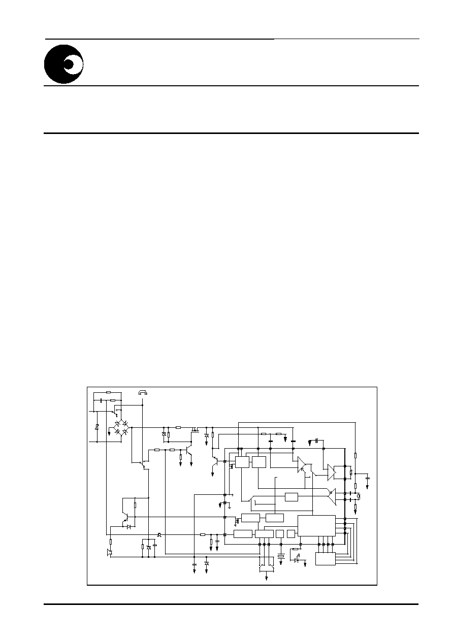
Block Diagram
General Description
The SA2532P is a CMOS integrated circuit that
contains all the functions needed to form a high
performance electronic telephone.
The device incorporates LD/MF repertory dialling,
melody generation, ring frequency discrimination
and a high quality speech circuit.
Soft switch into temporary MF mode using * when
LD mode is selected .Timed Break Recall will be
available in both LD and MF dialling modes.
A 31 digit Last Number Redial (LNR) memory, with
moving cursor protocol, activated by single key
depression.
Line Loss Compensation whereby send and receive
gains are adjusted (by 6dB) over the ranges
selected by the LLC pin.
KEYPAD
MODE_OUT
AGND
RI
STB
LS
LI
CS
DD
V
MO
SS
V
FC1
HS/DP
LLC
OSC
C1
C2
C3
C4
R1
R2
R3
R4
M2
M1
RO2
RO1
MUTE
SA2532P
DIALER
CLIP
SOFT
SENSE
CURRENT
LINE
Line Adaption
Power Extraction
DC Mask
GENERATOR
TONE
SEQUENCER
MELODY
RAM
OSC
LOGIC
CONTROL
DISCRIMINATION
FREQUENCY
RING
DD
V
+
+
+
+
+
+
hook
MODE
La
Lb
680n
5M1
2K2
20
100K
12V
BSS92
220K
150K
1M
10
BC327
30
300
1u
6K
CI
10u
510
100K
1N4148
330K
10u
18V
12V
330K
220K
10n
5V1
470u
Ringer
1K
2K2
1K8
100u
1K8
10n
10n
3.58MHz
2N5551
BC547B
4 x 1N4004
On
Off
Off
On
SA2532P
ONE MEMORY SINGLE
CHIP TELEPHONE

SA2532P
2 /21
sames
sames
sames
sames
Package
Available in 28 pin DIP.
1
2
3
4
5
6
7
8
9
10
11
12
13
14
15
16
17
18
19
20
21
22
23
24
25
26
27
28
LS
RO2
RO1
VDD
AGND
STB
CI
MO
LLC
HS/DP
OSC
RR
C4
C3
RI
LI
VSS
CS
M2
M1
MODE
FCI
R1
R2
R3
R4
C1
C2
SA2532P
Figure 1
SA2532P
3 /21
sames
sames
sames
sames
Pin Description
Pin #
Symbol
Function
23
24
M1
M2
Microphone Inputs
Differential inputs for the microphone (electret).
3
2
RO1
RO2
Receiver Outputs
These are the outputs for driving a dynamic ear piece with an impedance of
100 to 300Ohms
5
A
GND
Analog Ground
This is the analog ground for the amplifiers.
28
RI
Receive Input
This is the input for the receive signal.
6
STB
Side Tone Balance Input
This is the input for side tone cancellation.
1
LS
Line Current Sense Input
This is the input for sensing the line current.
27
LI
Line Input
This input is used for power extraction and line current sensing.
25
CS
Current Shunt Control Output
This N-channel open drain output controls the external high power shunt
transistor for the modulation of the line voltage and for shorting the line
during make period of pulse dialling.
4
V
DD
Positive Voltage Supply
This is the supply pin for the circuit.
26
V
SS
Negative Power Supply
8
MO
Melody Output
Pulse Density Modulated output of the melody generator for tone ringer. At
high impedance when not active.
21
FCI
Frequency Comparator Input
This is a Schmitt trigger input for ring frequency discrimination. Disabled
during off-hook.
10
HS/DPB
Hook Switch Input and Dial Pulse Output
This is an I/O that is pulled high by the hook switch when off- hook. An
open drain pulls it low during break periods of pulse dialling and flash.
11
OSC
Oscillator Input
Oscillator pin for Xtal or ceramic resonator (3.58 Mhz). Recommended :
Murata CSA 3.58MG312AM
12
RR
Repetition Rate.
Select pin for the repetition rate of the tone ringer's melody output.
9
LLC
Line Loss Compensation.
Select pin for the line loss compensation:
Open None
Low 20-50mA
High 45-75mA
SA2532P
4 /21
sames
sames
sames
sames
Pin Description Cont'd
Pin #
Symbol
Function
22
MODE
Signalling Mode Select Input
Mode pin Function
High LD default mode, make/break = 33/66 ms
Open MF only
Low LD default mode, make/break = 40/60 ms
20
19
18
17
R1
R2
R3
R4
Keyboard Rows
16
15
14
13
C1
C2
C3
C4
Keyboard Columns
7
CI
Complex Impedance Input
Input pin for the capacitor in the complex impedance
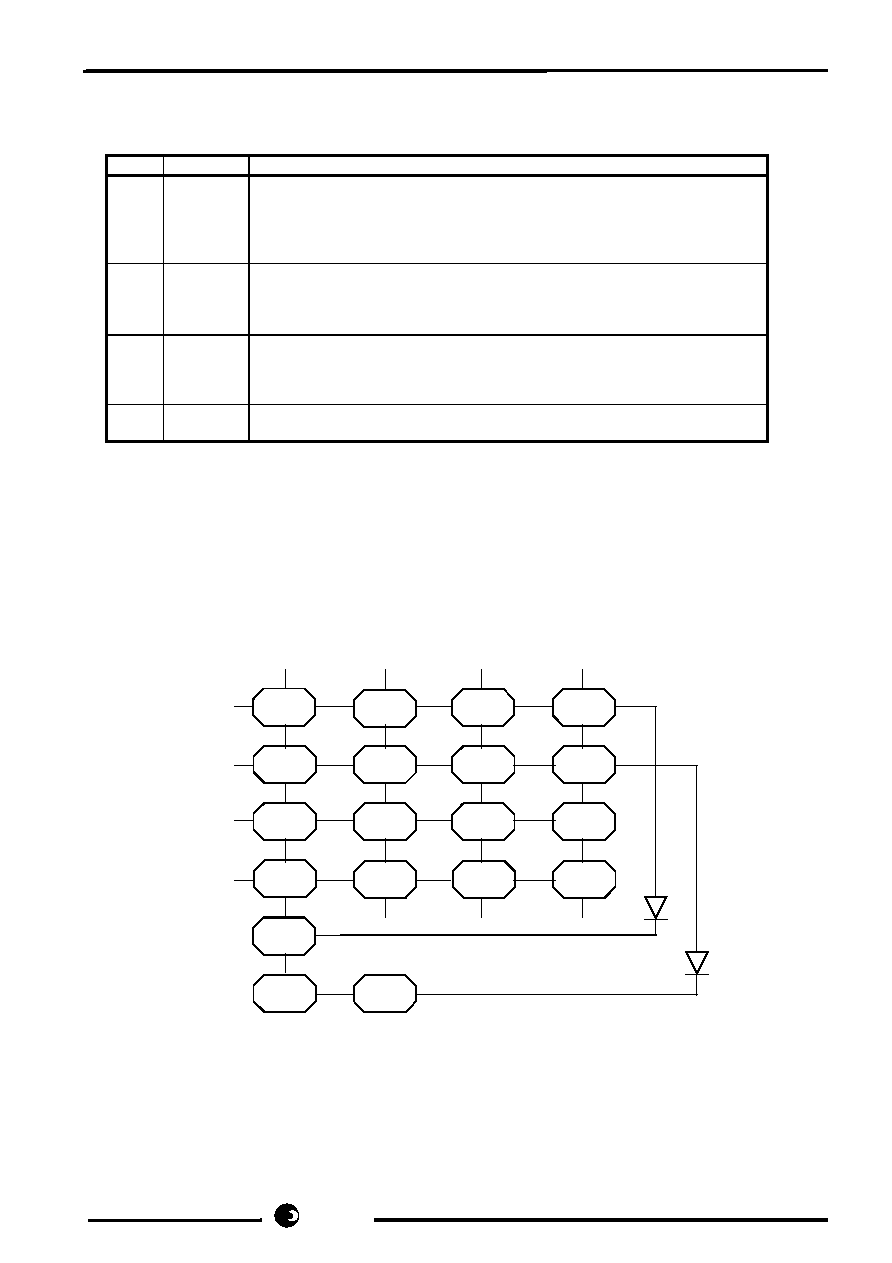
Keyboard Connections
MUTE
1
2
M5
8
7
6
5
4
3
0
R2
R
#
*
9
PAUSE
LNR
ENTER
C1
C2
C3
C4
R1
R2
R3
R4
Figure 2

SA2532P
5 /21
sames
sames
sames
sames
Power On Reset
The on chip power on reset circuit monitors the
supply voltage (V
DD
). When V
DD
rises above
approx. 1.2V, a power on reset occurs to assure
correct start-up and the LNR register is cleared
.
DC Conditions
The normal operating range is from 15mA to 100
mA. Operating range with reduced performance is
from 5mA to 15mA. In the operating range all
functions are operational. In the line hold range
from 0 to 5 mA the device is in a power down mode
and the voltage at LI is reduced to maximum 3.5V.
The dc characteristic (excluding diode bridge and
Pulsing transistors) is determined by the voltage at
LI and the resistor R1 as follows:
VLS = VLI + ILine.R1
The voltage at LI is 4.5V.
During pulse dialling the speech circuit and other
parts of the device not required are in a power
down mode to save current. The CS pin is pulled to
V
SS
in order to turn the external shunt transistor on
to keep a low voltage drop at the LS pin during
make periods.
AC Impedance
The Characteristic or Output impedance of the
SA2532P is set within the IC and adjusted to 600
Ohms. A capacitor may be added to the circuit at
pin CI to add a reactive element and make the
output impedance complex.
Oscillator
All the Timing Functions of the SA2532P are based
on a Clock Frequency of 3.58MHz. A ceramic
resonator of this frequency should be connected to
the OSC pin. In practice minor deviations from the
nominal frequency may occur due to the
characteristics of the frequency reference device
used and so it is recommended that care is taken in
the selection of components. Typically a small
value capacitor (
47pF) may be required to be
connected in parallel with the Frequency Reference
to ensure start-up and/or operation at the nominal
frequency.
Speech Circuit
The speech circuit consists of a transmit and a
receive path with soft clip, mute, line loss
compensation and side tone cancellation.
Transmit
The gain of the transmit path is 35 dB for M1/M2 to
LS (see test circuit in Figure 5). The microphone
input is differential with an input impedance of 25
kOhms. The soft clip circuit limits the output
voltage at LI to 2.0V
PEAK
. The attack time is
30us/6dB and the decay time is 20 ms/6 dB. When
mute is active, during dialling or after pressing the
MUTE key, the gain is reduced by > 60 dB.
Receive
The receive input is the differential signal of RI and
STB. The gain of the receive path is 2 dB (see test
circuit in Figure 5) with differential outputs,
RO1/RO2 . When mute is active during dialling the
gain is reduced by > 60dB. During DTMF dialling a
MF comfort tone is applied to the receiver. The
comfort tone is the DTMF signal with a level that is
-30dB relative to the line signal.
Side Tone
Side Tone is controlled along with Return Loss by a
Double Balance Bridge as shown in Figure 3. Good
sidetone cancellation is achieved by using the
following equation:
Z
bal
R5
------ = ----
Z
line
R1
The side tone cancellation signal is applied to the
STB input.
Line Loss Compensation
The line loss compensation is a pin selectable
option. When it is activated, the gains of the
transmit and receive amplifiers are changed by 6dB
in accord with the DC conditions as measured at
Pins LI and LS. When the LLC pin is low the
adjustment in gain occurs over the range I
LINE
= 20
to 50mA. When the LLC pin is high the gain range
is I
LINE
= 45 to 75mA.. Note that these values apply
for R1 = R30
. When LLC pin is open then the
amplifier gains remain fixed regardless of the line
current.