 | –≠–ª–µ–∫—Ç—Ä–æ–Ω–Ω—ã–π –∫–æ–º–ø–æ–Ω–µ–Ω—Ç: SA3488 | –°–∫–∞—á–∞—Ç—å:  PDF PDF  ZIP ZIP |
SA3488
sames
1
s
Actual input-output channel
connections stored and modified via
an on chip 8-bit parallel microprocessor
interface
s
6 main "Functions" or "Instructions"
available
s
Typical Bit Rate : 2Mbit/s
s
Typical Synchronization Rate : 8KHz
(time frame is 125µs)
s
5V power supply with internally
generated bias voltage
s
MOS & TTL input/output levels
compatible
sames
CMOS 256 X 256 DIGITAL SWITCHING MATRIX
SA3488
SA3488
s
Hardware (pin-to-pin) and software
compatible with M088 and M3488
s
256 input and 256 output channel digital
switching matrix
s
Building block designed for large
capacity electronic exchanges, sub-
systems and PABX
s
Non-blocking single stage and higher
capacity blocks (512 or 1024 channels)
s
European and U.S. standard
compatible (32/24 serial channels per
frame)
s
PCM inputs and outputs mutually
compatible
FEATURES
DESCRIPTION
The SA3488 is a non-blocking digital
switching matrix that is capable of routing
256 input channels to any of 256 output
channels. Data is fed into and out of the
device via eight serial PCM input and
output channels at 2MBits/sec. The device
can connect or disconnect each input
channel with any output channel, as well as
carry out other functions which are user
programmable via an eight bit parallel
microprocessor interface. The SA3488
sees its primary use as a building block in
high volume electronic exchanges, voice
data PABX and other standard data
communications applications. It can be
easily configured for operation in PCM 24
or PCM 30 formats.
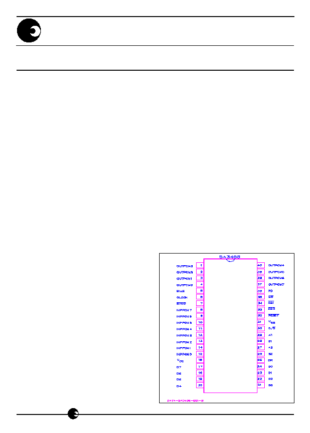
PIN CONNECTIONS:

SA3488
sames
2
BLOCK DIAGRAM

SA3488
sames
3
ABSOLUTE MAXIMUM RATINGS *
Symbol
Parameter
Value
Unit
V
CC
Supply Voltage
-0.3 to 7
V
V
I
Input Voltage
-0.3 to 7
V
V
O
Off State Output
7
V
P
tot
Total Package Power Dissipation
1.5
W
T
stg
Storage Temperature Range
-40 to +125
∞C
T
op
Operating Temperature Range
0 to +70
∞C
* Stresses above those listed under "Absolute Maximum Ratings" may cause permanent damage
to the device. This is a stress rating only. Functional operation of the device at these or any other
condition above those indicated in the operation sections of this specification, is not implied.
Exposure to Absolute Maximum Ratings for extended periods may affect device reliability.
RECOMMENDED OPERATING CONDITIONS
Symbol
Parameter
Value
Unit
V
CC
Supply Voltage
4.75 to 5.25
V
V
I
Input Voltage
0 to 5.25
V
V
O
Off State Input Voltage
0 to 5.25
V
CLOCK Freq.
Input Clock Frequency
4.096
MHz
SYNC Freq.
Input Synchronization
8
KHz
T
op
Operating Temperature
0 to 70
∞C
CAPACITANCES (Measuring freq. = 1MHz; T
op
= 0 to 70∞C; unused pins tied to V
SS
)
Symbol Parameter
Pins
Min. Typ. Max. Unit
C
I
Input Capacitance
6 to 15; 26 to 30; 32 to 36
5
pf
C
I/0
I/O Capacitance
20 to 24
15
pf
C
0
Output Capacitance 1 to 4; 17 to 19; 37 to 40
10
pf
SA3488
sames
4
D.C. ELECTRICAL CHARACTERISTICS (T
amb
= 0 to 70∞C, V
CC
= 5V 5%)
All D.C. characteristics are valid 250µs after V
CC
and clock have been applied.
Symbol Parameter
Pins
Test Condition
Min. Typ. Max. Unit
V
ILC
Clock Input Low Level
6
-0.3
0.8
V
V
IHC
Clock Input High Level
6
2.4
V
CC
V
V
IL
Input Low Level
7 to 15
-0.3
0.8
20 to 24
V
26 to 30
32 to 36
V
IH
Input High Level
7 to 15
2.0
V
CC
20 to 24
V
26 to 30
32 to 36
V
OL
Output Low Level
17 to 25
I
OL
= 1.8mA
0.4
V
V
OH
Output High Level
17 to 25
I
OH
= 250µA
2.4
V
V
OL
PCM Output Low Level
1 to 4
I
OL
= 2.0mA
0.4
V
37 to 40
I
IL
Input Leakage Current
6 to 15
V
IN
= 0 to V
CC
10
µA
26 to 30
32 to 36
I
DL
Data Bus Leakage
17 to 24
V
IN
= 0 to V
CC
±10
µA
Current
V
CC
applied; Pins 35
and 36 tied to V
CC
, after
Device Initialization
I
CC
Supply Current
16
Clock Freq.= 4.096MHz
180
mA

SA3488
sames
5
A.C. ELECTRICAL CHARACTERISTICS (T
amb
= 0 to 70∞C, V
CC
= 5V ±5%)
All A.C. characteristics are valid 250µs after V
CC
and clock have been applied. C
L
is the max.
capacitive load and R
L
the test pull up resistor.
Signal
Symbol Parameter
Test Condition
Min.
Typ. Max. Unit
CK
t
CK
Clock Period
230
ns
(clock)
t
WL
Clock Low Level Width
100
ns
t
WH
Clock High Level Width
100
ns
t
R
Rise Time
25
ns
t
F
Fall Time
25
ns
SYNC
t
SL
Low Level Setup Time
80
ns
t
HL
Low Level Hold Time
40
ns
t
SH
High Level Setup Time
80
ns
t
WH
High Level Width
t
CK
ns
PCM input
t
S
Setup Time
-5
ns
Busses
t
H
Hold Time
45
ns
PCM
t
PDmin
Propagation time
CL = 50pf,R
L
=2K
45
ns
Output
referred to CK low level
Busses
t
PDmax
Propagation time
CL = 50pf,R
L
=2K
200
ns
referred to CK high level
RESET
t
SL
Low Level Setup Time
100
ns
t
HL
Low Level Hold Time
50
ns
t
SH
High Level Setup Time
90
ns
t
WH
High Level Width
t
CK
ns
WR
t
WL
Low Level Width
150
ns
t
WH
High Level Width
t
CK
ns
t
REP
Repetition Interval
t
REP
= 40+2 t
CK +
see
between Active Pulses
+ t
WL(CK) +
formula
t
SH
High Level Setup Time
+ t
R(CK)
0
ns
to Active Read Strobe
t
HH
High Level Hold Time
20
ns
from Active Read Strobe
t
R
Rise Time
60
ns
t
F
Fall Time
60
ns
RD
t
WL
Low Level Width
180
ns
t
WH
High Level Width
t
CK
ns
t
REP
Repetition Interval
t
REP
= 40+2 t
CK
see
between Active Pulses
+ t
WL
+ t
R
formula
t
SH
High Level Setup Time
0
ns
to Active Read Strobe
t
HH
High Level Hold Time
20
ns
from Active Write Strobe
t
R
Rise Time
60
ns
t
F
Fall Time
60
ns

SA3488
sames
6
A.C. ELECTRICAL CHARACTERISTICS (Cont.)
Signal
Symbol
Parameter
Test Conditions
Min. Typ.
Max. Unit
CS1,
t
SL(CS-WR)
Low level setup time
Active Case
0
ns
CS2
to WR falling edge
t
HL(CS-WR)
Low level hold time
Active Case
0
ns
from WR rising edge
t
SH(CS-WR)
High level setup time
Inactive Case
0
ns
to WR falling edge
t
HH(CS-WR)
High level hold time
Inactive Case
0
ns
from WR rising edge
t
SL(CS-RD)
Low level setup time
Active Case
0
ns
to RD falling edge
t
HL(CS-RD)
Low level hold time
Active Case
0
ns
from RD rising edge
t
SH(CS-RD)
High level setup time
Inactive Case
0
ns
to RD falling edge
t
HH(CS-RD)
High level hold time
Inactive Case
0
ns
from RD rising edge
C/D
t
S(C/D-WR)
Setup time to write
strobe end
130
ns
t
H(C/D-WR)
Hold time from
write strobe end
25
ns
t
S(C/D-WR)
Setup time to read
strobe start
20
ns
t
H(C/D-WR)
Hold time from read
strobe end
25
ns
A1,S1,
t
S(match-WR)
Setup time to write
130
ns
A2,S2
strobe end
(match
t
H(match-WR)
Hold time from
25
ns
inputs)
strobe end
t
S(match-RD)
Setup time to read
20
ns
strobe start
t
H(match-RD)
Hold time from read
25
ns
strobe end
DR
t
W
Low state width
Instructions 5,6
2 t
CK
ns
(data
t
PD
DR output delay
ready)
from write strobe end
Instructions 5,
5.t
CK
14 t
CK
(active command)
C
L
= 50pf
ns

SA3488
sames
7
D0 to D7
t
S(BUS-WR)
Input setup time to
130
ns
(Interface
write strobe end
bus)
t
H(BUS-WR)
Input hold time
25
ns
from write strobe end
t
PD(BUS)
Propagation time
C
L
= 200pf
120
ns
from (active) falling
edge of read strobe
t
HZ(BUS)
Propagation time
80
ns
from (active)rising
edge of read strobe
to high impedance
state
A.C. ELECTRICAL CHARACTERISTICS (Cont.)
Signal
Symbol
Parameter
Test Conditions
Min. Typ.
Max. Unit

SA3488
sames
8
PIN DESCRIPTION
Pin
Designation
Description
17
D7
Bidirectional data bus used to transfer data and instructions
18
D6
to and from the microprocessor. The output bus is 8 bits
19
D5
wide and the input 5 bits wide. D0 is the least significant
20
D4
digit. The bus is tristate and is not available for use while
21
D3
RESET is held low.
22
D2
23
D1
24
D0
30
C/D
In a write operation C/D = 0 qualifies bus content as data,
while C/D = 1 qualifies it as a opcode. In a read operation
C/D = 0 selects OR1 whereas C/D = 1 selects OR2.
33
CS2
Chip select pins. Enable the device to perform valid read
34
CS1
and write operations (active low). The two pins allow for
row column selection for different types of microprocessors;
normally though one is tied low.
26
S2
Address select or match pins. With S1 and S2 hardwired
27
A2
to ground or V
CC
, signals on A1 and A2 give rise to a 28S1
matched or unmatched condition i.e. S1=A1, S2=A2 =>a
29
A1
matched condition. Since in a matrix structure, devices in
the same row share the same PCM output bus, instructions
pertaining to channel connections (matched condition),
must be processed as channel disconnections in the other
devices (unmatched condition). Two channels can
therefore never collide.
35
WR
When CS1 and CS2 are low, WR enables data transfer
from the microprocessor to the device. Data, opcode and
control signals are latched on the rising edge of WR. To
ensure simultaneous instruction execution in a multichip
configuration the WR rising edge must be 20 to 20 + t
WL(CK)
nsec late relative to the clock falling edge.
36
RD
When CS1 and CS2 are low and a matched condition
exists, a low level on RD enables OR1 or OR2 for a read
operation. In addition the rising edge of RD latches C/D
and the matched condition pins in order to direct the
internal
flow of operations. In a multichip configuration
the same timing requirement must be met as in the WR
case.
SA3488
sames
9
Pin Description (Cont.)
Pin
Designation
Description
32
RESET
This pin is used to initialise the device. The initialisation
routine takes one time frame whatever the RESET pulse
width (one clock cycle minimum). All internal registers are
set 'high' and the control memory is set to all 'ones' i.e.
channel disconnection. The data bus is pulled to a high
impedance state as well as the PCM output channels.
25
DR
DR is the data ready pin which is normally high. If DR goes
low the following information is available via this pin.
1. Invalid instruction code (The pin is held low until a valid
instruction is loaded).
2. An active output channel was found in a matrix of
devices with the same CS pins during the execution of
instruction 5. DR is low for two clock cycles.
3. Status register 2 was loaded with the total number of
messages in time slot 0 during the execution of
instruction
6. DR is active low for two clock cycles.
6
CLOCK
Input clock frequency is typically 4.096Mhz. This signal
will set the internal input/ output channel bit rate to 2.048
Mbits/sec. The bit rate is set by division of the master
clock frequency.
7
SYNC
The input synchronisation signal frequency is 8kHz and is
active low. Internally generated time bases that maintain
sequential addressing are synchonised via the SYNC
signal.
8
INP PCM7
The input PCM bus accepts a standard data rate of 2MBits/
sec.
9
INP PCM6
10
INP PCM5
11
INP PCM4
12
INP PCM3
13
INP PCM2
14
INP PCM1
15
INP PCM0

SA3488
sames
10
Pin Description (Cont.)
Pin
Designation
Description
37
OUT PCM7
Output PCM channel bit rate is also 2MBits/sec. The
output
38
OUT PCM6
buffers are open drain simulating a wired
OR connection.
39 OUT PCM5 This minimises current spike problems in
multichip
40 OUT PCM4 configurations. Input and output channels
are driven in
1 OUT PCM3 such a manner as to reduce any analogue
delay time up to:
2
OUT PCM2
Time delay max = 1 bit time-(clock high prop. time - Clock
3
OUT PCM1
low prop. time).
4
OUT PCM0
5
BIAS
Internally generated bias voltage (-2.5 to -3.0V for V
CC
in
the operating range). A maximum of 220pf capacitor
connected to pin 5 provides improved filtering.

SA3488
sames
11
FUNCTIONAL OVERVIEW
The SA3488 is intended for large telephone switching systems, mainly central exchanges,
digital line concentrators and private branch exchanges where a distributed microcomputer
control approach is extensively used. It consists of a speech memory (SM), a control
memory (CM), a serial/parallel and a parallel/serial converter, an internal parallel bus,
an interface (8 data lines, 11 control signals) and dedicated logic. By means of repeated
clock division two time bases are generated. These are preset from an external
synchronization signal to two specific count numbers so that sequential scanning of the
bases give synchronous addresses to the memories and I/O channel controls. Different
preset count numbers are needed because of processing delays and data path direction.
The time-base for output channels is advanced with respect to the actual time. Each
serial PCM input channel is converted to parallel data and stored in the speech memory
at the beginning of any new time slot (according to first timebase) in the location
determined by input pin number and time slot number. The control memory CM
maintains the correspondences between input and output channels. More exactly, for
any output pin/output channel combination the control memory gives either the full
address of the speech memory location involved in the PCM transfer or an 8-bit word to
be supplied to the parallel/serial output converter. A 9
th
bit at each CM location defines
the data source for output links; low for SM, high for CM.
The late timebase is used to scan the output channels and to determine the pins to be
serviced within each channel. Enough idle cycles are left to the microprocessor for
synchronous instruction processing. Two 8-bit registers OR1 and OR2 supply feedback
data for control or diagnostic purposes; OR1 comes from the internal bus i.e. from
memories, while OR2 gives an opcode copy and additional data to the microcomputer.
A four byte, 5-bit stack register and an instruction register, under microcomputer
control,
store input data available at the interface.
Dedicated logic, under control of the microprocessor interface, extracts the 0 channel
content of any selected PCM input bus, using spare cycles of SM.

SA3488
sames
12
FUNCTIONAL DESCRIPTION OF SPECIFIC MICROPROCESSOR OPERATIONS
The device, under microprocessor control, performs the following instructions:
1
CHANNEL CONNECTION/DISCONNECTION
2
CHANNEL DISCONNECTION
3
INSERTION OF A BYTE ON A PCM OUTPUT CHANNEL/CHANNEL
DISCONNECTION)
4
TRANSFER OF A SINGLE OUTPUT CHANNEL SAMPLE
5
TRANSFER OF A SINGLE OUTPUT CHANNEL CONTROL WORD
6
TRANSFER OF SELECTED 0 CHANNEL PCM INPUT DATA ACCORDING TO AN
8-BIT MASK PREVIOUSLY STORED IN THE "EXPECTED MESSAGES"
REGISTER.
The instruction flow is as follows:
Any input protocol is started by the microprocessor interface loading the internal stack
register with 2 bytes (4 bytes for instructions 1 and 3) qualified as data bytes by C/D =
0 and a specific opcode qualified by C/D = 1 (match condition is normally needed).
After the code is loaded, the instruction register is immediately checked to see whether
it is acceptable; if not, it is rejected. If accepted the instruction is also processed as
regards match condition and is appended for execution during the memories' space
cycles.
Four cases are possible:
a)
the code is not valid; execution cannot take place, the DR output pin is reset to
indicate the error and all registers are saved;
b)
the code is valid for types 2, 4 and 6 but it is unmatched; execution cannot take place,
and DR is not affected.
c)
the code is valid for types 1 and 3 and it is unmatched; the instruction is interpreted
as a channel disconnection.
d)
the code is valid and it either matches or is of type 5; the instruction is processed as
received.
Validation control takes only two cycles out of a total execution time of 5 to 13 cycles;
the last operation is the updating of the contents of registers OR1 and OR2.

SA3488
sames
13
During a very long internal operation (device initialization after RESET going high or
execution of instruction 6) a new set of data bytes with a valid opcode is accepted while
a wrong code is rejected. At the end of the current routine execution takes place in the
same way as described before.
At the end of an instruction it is normally recommended to read one or both registers. To
enable instruction 6, however, it is necessary to read register OR2. This is because
instruction 6, used between other short instructions of type 1 to 5, must have a lower
priority and can be enabled only after the short instructions have been completed.
Instruction 6 normally has a long process and a special flow which is described below.
First a not-all-zero mask is stored in the "expected messages" register and in another
"background" register. This operation starts the second phase of instruction 6 which is
called "channel 0 extraction" and is repeated at the beginning of any new time frame. At
the beginning of the time frame a new copy of activated channels to be extracted is made
from the "background register" and put in the "expected messages" register. In addition
the latter register is modified to indicate the exact number of messages that have arrived.
The term messages covers any input 0 channel data with starting sequence different
from the label 01. So using this label the number of expected messages can be reduced
to correspond to the number of effective messages. If and only if the residual number
is different from zero will the device start the extraction protocol at the end of the current
routine.
The procedure is as follows: the DR output is pulsed low as a two cycle interrupt request
and OR2 is loaded with the total number of active channels to be extracted.
The transfer of OR2 contents to the microprocessor continues the extraction which
consists of repeated steps of OR1 and OR2 loading, indicating respectively the message
and the incoming bus number. Reading the registers in the order OR1, OR2 must be
continued until completion or until the time frame runs out.
With a new time frame a new extraction process begins, resuming the copy operation
from the background register.
During extraction the active channels are scanned from the highest to the lowest number
(from 7 to 0). While extraction is being carried out the time interval requirements between
active rising edges of RD are a minimum of 5 to 13 t
CK
for sequence OR2 - OR1 and a
minimum of 3 times t
CK
for sequence OR1 - OR2. More details are given in the following
tables.

SA3488
sames
14
INSTRUCTION TABLES
The most significant digits of OR2 A7, A6, A5 are a copy of the PCM selected output bus;
the least significant digits or OR2 are the opcode while C8 is the control bit. In all cases
parentheses () define actual register contents.
INSTRUCTION 1: CHANNEL CONNECTION/DISCONNECTION
Control Signals
Data Bus
Match C/D CS
WR RD
D7
D6
D5
D4
D3
D2
D1
D0
Notes
X
0
0
0
1
X
X
X
X
X
Bi2
Bi1
Bi0
1
st
Data Byte:selected input bus
X
0
0
0
1
X
X
X
Ci4
Ci3
Ci2
Ci1
Ci0
2
nd
Data Byte: selected input
channel
X
0
0
0
1
X
X
X
X
X
Bo2 Bo1 Bo0 3
rd
Data Byte: selected output
bus
X
0
0
0
1
X
X
X
Co4 Co3 Co2 Co1 Co0 4
th
Data Byte: selected output
channel
Yes/No 1
0
0
1
X
X
X
X
0
0
0
1
Instruction Opcode
Yes
0
0
1
0
C7
C6
C5
C4
C3
C2
C1
C0
0R1 : CM content copy,
(1
1
1
1
1
1
1
1)
that is for mismatch
(Bi2 Bi1
Bi0
Ci4
Ci3
Ci2
Ci1
Ci0) condition or match
condition
Yes
1
0
1
0
A7
A6
A5
C8
0
0
0
1
OR2
(Bo2 B01 Bo0 1
0
0
0
1)
(Bo2 Bo1 Bo0 0
0
0
0
1)
INSTRUCTION 2: OUTPUT CHANNEL DISCONNECTION
Control Signals
Data Bus
Match C/D CS
WR RD
D7
D6
D5
D4
D3
D2
D1
D0
Notes
X
0
0
0
1
X
X
X
X
X
Bo2 Bo1 Bo0 1
st
Data Byte: selected output
bus
X
0
0
0
1
X
X
X
Co4 Co3 Co2 Co1 Co0 2
nd
Data Byte: selected
output channel
Yes
1
0
0
1
X
X
X
X
0
0
1
0
Instruction Opcode
Yes
0
0
1
0
1
1
1
1
1
1
1
1
OR1 : CM Content Copy
(output channel is inactive)
Yes
1
0
1
0
A7
A6
A5
1
0
0
1
0
OR2
(Bo2 Bo1 Bo0 1
0
0
1
0)
SA3488
sames
15
INSTRUCTION 3: LOADING A MICROPROCESSOR BYTE
Control Signals
Data Bus
Match C/D CS
WR RD
D7
D6
D5
D4
D3
D2
D1
D0
Notes
X
0
0
0
1
X
X
X
X
X
Ci7
Ci6
Ci5
1
st
Data Byte: most significant
digits to be inserted
X
0
0
0
1
X
X
X
Ci4
Ci3
Ci2
Ci1
Ci0
2
nd
Data Byte: least significant
digits to be inserted
X
0
0
0
1
X
X
X
X
X
Bo2 Bo0 Bo1 3
rd
Data Byte: selected output
bus
X
0
0
0
1
X
X
X
Co4 Co3 Co2 Co1 Co0 4
th
Data Byte: selected output
channel
Yes/no 1
0
0
1
X
X
X
X
0
1
0
0
Instruction Opcode
Yes
0
0
1
0
C7
C6
C5
C4
C3
C2
C1
C0
OR1 : CM
(1
1
1
1
1
1
1
1)
content copy, that
(Ci7 Ci6
Ci5
Ci4
Ci3
Ci2
Ci1
Ci0) is for mismatch condition or
match condition
Yes
1
0
1
0
A7
A6
A5
1
0
1
0
0
OR2
(Bo2 Bo1 Bo0 1
0
1
0
0)
INSTRUCTION 4: TRANSFER OF A SINGLE PCM SAMPLE
Control Signals
Data Bus
Match C/D CS
WR RD
D7
D6
D5
D4
D3
D2
D1
D0
Notes
X
0
0
0
1
X
X
X
X
X
Bo2 Bo1 Bo0 1
st
Data Byte: selected output
bus
X
0
0
0
1
X
X
X
Co4 Co3 Co2 Co1 Co0 2
nd
Data Byte: selected output
channel
Yes
1
0
0
1
X
X
X
X
1
0
1
1
Instruction Opcode
Yes
0
0
1
0
C7
C6
C5
C4
C3
C2
C1
C0
OR1 : CM Content
S7
S6
S5
S4
S3
S2
S1
S0
Copy if C8= 1; or
SM Content Sample if C8=0
Yes
1
0
1
0
A7
A6
A5
C8
1
0
1
1
OR2
(Bo2 Bo1 Bo0 C8
1
0
1
1)
Note: S7..S0 is a parallel copy of the PCM data; S7 is the most significant digit and the first of the sequence.
SA3488
sames
16
INSTRUCTION 5: TRANSFER OF AN OUTPUT CHANNEL CONTROL WORD
Control Signals
Data Bus
Match C/D CS
WR RD
D7
D6
D5
D4
D3
D2
D1
D0
Notes
X
0
0
0
1
X
X
X
X
X
Bo2 Bo1 Bo0 1
st
Data Byte: selected output
bus
X
0
0
0
1
X
X
X
Co4 Co3 Co2 Co1 Co0 2
nd
Data Byte: selected output
channel
X
1
0
0
1
X
X
X
X
1
0
0
0
Instruction Opcode
Yes
0
0
1
0
C7
C6
C5
C4
C3
C2
C1
C0
OR1 : CM selected CM word
copy
Yes
1
0
1
0
A7
A6
A5
C8
1
0
0
0
OR2
(Bo2 Bo1 Bo0 C8
1
0
0
0)
INSTRUCTION 6: CHANNEL 0 SELECTION MASK STORE/DATA TRANSFER
Control Signals
Data Bus
Match C/D CS
WR RD
D7
D6
D5
D4
D3
D2
D1
D0
Notes
X
0
0
0
1
X
X
X
X
X
Mi7 Mi6
Mi5
1
st
Data Byte: most significant
digits of selection mask
X
0
0
0
1
X
X
X
Mi4
Mi3
Mi2 Mi1
Mi0
2
nd
Data Byte: most significant
digits of selection mask
Yes
1
0
0
1
X
X
X
X
1
1
1
0
Instruction Opcode
Mask store control
Yes
0
0
1
0
(previous content)
OR1 : register is not affected
Yes
1
0
1
0
N2
N1
N0
Tn
1
1
1
0
OR2 : see below
First Data Transfer (after DR going low)
Yes
0
0
1
0
(previous content)
OR1 : register is not affected
Yes
1
0
1
0
N2
N1
N0
Tn
1
1
1
0
OR2 : see below
Repeated Data Transfer (after first OR2 transfer)
Yes
0
0
1
0
S7
S6
S5
S4
S3
S2
S1
S0
OR1 : expected message stored
in SM
Yes
1
0
1
0
P2
P1
P0
Fn
1
1
1
0
OR2
Notes: 1.
Regarding mask bits Mi0 to Mi7 a logic "0" level means disabling condition, a logic "1" level means
enabling condition.
2.
A null mask or a RESET pulse clears the mask and the deep background mask registers and disable
channel 0 extraction function.
3.
Reading of OR2 is optional after mask store or redefinition, because function is activated only by not-
null mask writing.
4.
After mask store (N2 N1 N0) is the sum of activated channels, after DR is the sum of active channels;
Tn=1/0 means activation/suppression of the function after store while after DR only Tn = 1 can appear
indicating non-null configuration extraction.
5.
Reading of OR2 is imperative after DR in order to step the data transfer; reading of OR1 is also needed
to scan in descending order the priority register. Relevant messages only are considered, i.e. only
messages with a MSD label different from 0 1.
6.
(P2 P1 P0) is the PCM bus on which the message copied in OR1 was found; Fn is a continuation bit
telling respectively on level 1/0 for any more/no more extraction to be
performed.
SA3488
sames
17
PCM TIMING, RESET
WRITE OPERATION TIMING

SA3488
sames
18
READ OPERATION TIMING

SA3488
sames
19
Notes:

SA3488
sames
20
Any Sales or technical questions may be posted to our e-mail address below:
energy@sames.co.za
For the latest updates on datasheets, please visit out web site:
http://www.sames.co.za
South African Micro-Electronic Systems (Pty) Ltd
P O Box 15888,
33 Eland Street,
Lynn East, 0039
Koedoespoort Industrial Area,
Republic of South Africa,
Pretoria,
Republic of South Africa
Tel:
012 333-6021
Tel:
Int +27 12 333-6021
Fax:
012 333-8071
Fax:
Int +27 12 333-8071
Disclaimer:
The information contained in this document is confidential and proprietary to South African Micro-
Electronic Systems (Pty) Ltd ("SAMES") and may not be copied or disclosed to a third party, in whole or in part,
without the express written consent of SAMES. The information contained herein is current as of the date of
publication; however, delivery of this document shall not under any circumstances create any implication that the
information contained herein is correct as of any time subsequent to such date. SAMES does not undertake to
inform any recipient of this document of any changes in the information contained herein, and SAMES expressly
reserves the right to make changes in such information, without notification,even if such changes would render
information contained herein inaccurate or incomplete. SAMES makes no representation or warranty that any
circuit designed by reference to the information contained herein, will function without errors and as intended by
the designer.