
FEATURES
n
Drives 24 LED's under control of Serial
Interface
n
Light Emitting Diode intensity
programmable using a single resistor
n
Automatic lamp test facility on reset
(MRST)
n
Minimal external components
n
LED intensity constant, regardless of
number of LED's illuminated
sames
PDS039-SA8803-001 REV. C 07-03-96
LIGHT EMITTING DIODE DRIVER
4159
SA8803
1/10
n
11 Bit Information word controls up to
192 LED's (using eight SA8803s)
n
Readback of LED status
n
Requires a local clock of 8 times the
data rate
n
Constant current from power supply
option
DESCRIPTION
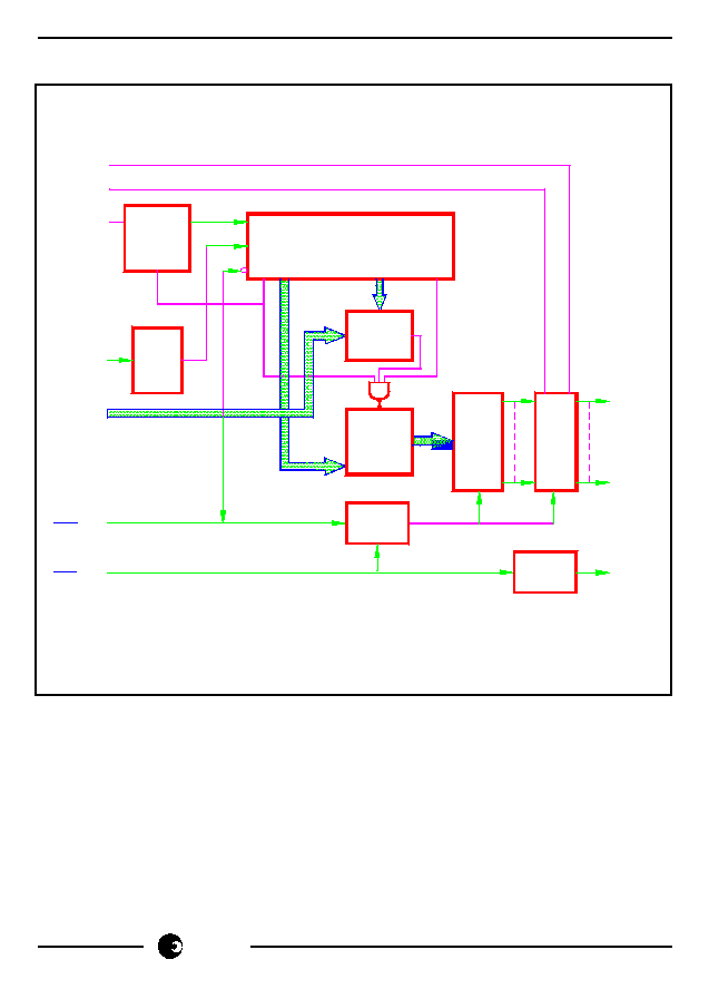
The block Diagram of the SA8803 is shown in
Fig. 1. A control word is clocked into the
device via the DATA pin with a local clock
provided to pin CLK. The control word
comprises a 3-bit chip address, a 5-bit LED
address and a Status (on/off) bit. Provided
that the Chip Adress matches the setting on
pins AD0..AD2 then the LED State Register is
addressed and the state of the selected LED
is set according to the Status bit in the Control
word.
The LEDs are driven by banks of Constant
Current Sources in which the value of the
current in all six banks is set by a single
external resistor connected between pin
INTENS and VEE. The total current drained
by the device and the LEDs may be fixed at
six times the LED current by connecting pin
CC to GND.
The status of all LEDs can be verified at any
time by pulling the TEST pin low. When tis
happens the contents of the LED Status
Register are clocked out of the SA8803 on the
pin DOUT. An additional test feature is that
al LEDs are illuminated for a short period after
power up to simplify system testing.
PIN CONNECTIONS
23
V
DD
SA8803
1
AD 0
LED 7
DR-00593
LED 8
LED 9
V DD
LED 11
V
EE
LED 10
18
19
15
16
17
INTENS
LED 12
20
21
22
V EE
LED 4
LED 5
LED 6
LED 1
LED 2
LED 3
V
CC
DOUT
AD 2
AD 1
10
11
12
13
14
7
8
9
6
5
4
3
2
DD
LED 19
LED 13
LED 14
LED 15
24
25
26
V
EE
LED 16
27
28
29
30
31
V
LED 18
LED 17
DD
DATA
GND
MRST
CLK
N.C.
44
43
42
32
33
34
35
36
37
38
39
41
40
V
LED 21
LED 20
EE
LED 22
TEST
LED 24
LED 23
SA8803
sames
2/10
FIGURE 1: BLOCK DIAGRAM
11 - BIT SHIFT REGISTER
DR-00594
AD0....AD2
MRST
TEST
START
BIT
DETECTION
CLOCK
SYNC
INTENS
CLK
CC
DATA
SIN
CLK
RESET
START
BIT
S CLK
LED
SELECTION
BUS
LED1
RESET
LAMP TEST
LOGIC
LED
ADDRESS
DECODER
24-BIT
LED
STATE
REGISTER
TEST
CONTROL
LOGIC
LED
DRIVERS
DOUT
LED24
3-BIT
CHIP
ADDRESS
COMPARATOR
STOP
BIT
SA8803
sames
3/10
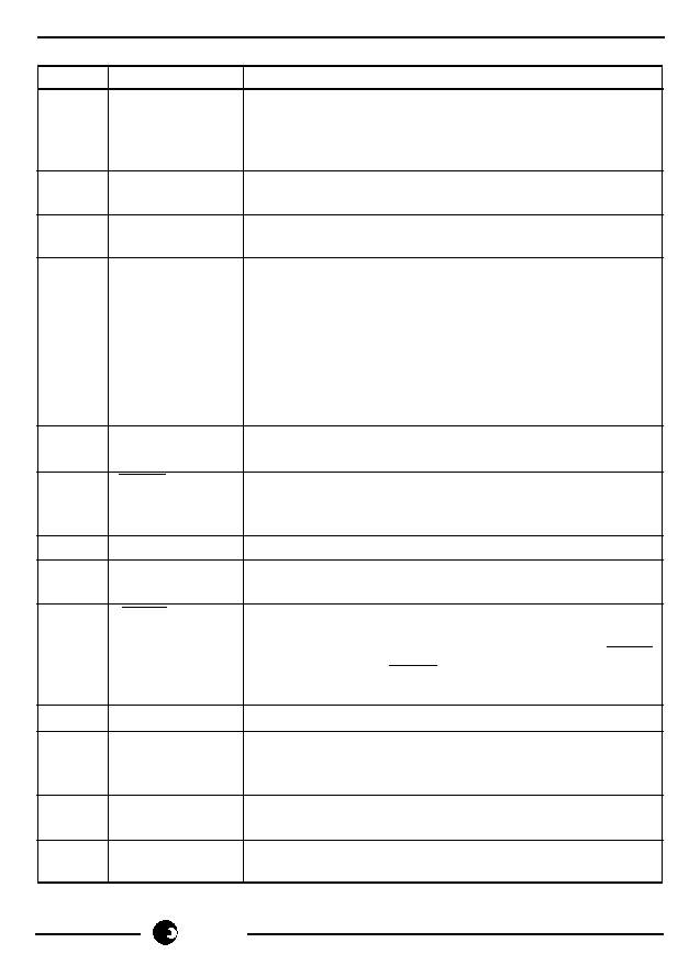
Pin
Designation
Description
1..3
AD0..AD2
Device address input pins. The binary code set up on
these pins, must match the address field of the control
word, before device access may be achieved. These
Schmitt-triggered inputs have on-chip pull-up resistors.
4
DOUT
This output is used for the manufacturers test requirements
and MUST be left open.
5
CC
Constant Current Drain Select.This Schmitt-triggered
input has on-chip pullup provided.
7..10,
LED1..LED4,
High current LED drive terminal outputs.
12..14,
LED5..LED7
16..18,
LED8..LED10,
20..21,
LED11..LED12,
24..26
LED13..LED15,
28..30
LED16..LED18,
32..34,
LED19..LED21,
36..38
LED22..LED24
22
INTENS
This analog input is used to set the drive current supplied
to the LED's. A resistor is connected from this pin to V
EE
.
39
TEST
Active low input that enables the internal LED status word
to be output from the DOUT pin. This Schmitt-triggered
input has on-chip pullup provided.
40
NC
Internally Unconnected.
41
CLK
External clock Schmitt-triggered input runs at 8X the data
rate (Baud rate).
42
MRST
This active low Schmitt-Trigger input may be used to
reset all internal registers. When active (low) this input
will cause all LED's to be driven for the duration of MRST
(lamp test). When MRST goes inactive all LED's will be
turned off. On-chip pullup provided.
43
GND
0V Supply Input for logic (0V)
44
DATA
Serial data input. Accept data in the form of an 11-bit
information word. This Schmitt-triggered input has on-
chip pullup provided.
11, 19,
VEE
Negative Supply Inputs (-5V)
27, 35
6, 15,
VDD
Positive Supply Inputs (+5V)
23, 31
Note: All inputs and outputs are CMOS compatible, unless otherwise specified.
PIN DESCRIPTION
SA8803
sames
4/10
FUNCTIONAL DESCRIPTION
1.
Control Word
The control word written serially into the DATA pin, will contain 9 information bits.
The data structure is illustrated in Figure 2 below.
Because the chip address is 3 bits wide, a single chip controller will be able to
address 8 SA8803 devices. Each SA8803 can drive 24 LED's, which means that
the controller is capable of addressing 192 LED's. The address bits in the control
word are internally compared with the address on the AD0..AD2 address lines to
determine if the SA8803 is being addressed.
Table 1. LED Addresses
L5
L4
L3
L2
L1
LED
0
0
0
0
0
IGNORED
0
0
0
0
1
1
0
0
0
1
0
2
etc
1
1
0
0
0
24
1
1
0
0
1
IGNORED
1
1
1
1
1
FIGURE 2: CONTROL WORD STRUCTURE
9-BIT CONTROL WORD
LED BIT ADDRESS INSIDE BANK
DEVICE BIT ADDRESS
STATUS BIT
S
=
DR-00595
=
=
=
=
L1
SB
E
SB
A0 ... A2
L1 ... L5
START BIT
END BIT
L2
L3
L4
A1
L5
S
A0
E
SB
A2
As can be seen from the structure of the control word, the controller should send 1
start bit, 9 data bits, and 1 stop bit.
When a LED is addressed its state will be set according to the status bit. A logic
one will enable the LED, and a logic zero will disable the LED.

SA8803
sames
5/10
4.
Constant Current Mode
When the CC pin is pulled high, the device will draw a constant current from the V
DD
supply which is equal to all LED's in the "on"condition regardless of the status of the
LED's.
5.
Clock Characteristics
S
CLK
is the internal synchronous clock derived from the asynchronous external clock
applied at the CLK input pin. It divides the external clock by 8. Theoretically the
rising edge of S
CLK
(synchronous Clock) should be in the middle of every bit, as
shown in Figure 4. Because of phase shift due to the clock frequency being more
or less than 8 times the baud rate, this edge may shift its position with regard to the
bit period (B
P
). The extreme case that may still be tolerated is an edge arriving at
either the beginning, or end of bit 11. This represents the maximum shift that can
be tolerated for valid data to be received for an inaccurate input clock frequency
(F
O
).
V
X
R
3.
LED Intensity Control
The LED "on" current (I
D
), is determined by the current flowing from the INTENS pin
through the external resistor. The values of I
D
can be calculated as follows:
I
D
= K
T
.
K
T
- Current Transfer Ratio of the Internal Current Mirror (typically 10.0)
R - The programming resistor value
V
X
- The voltage drop across the external resistor (internally controlled to 5.0V)

SA8803
sames
6/10
The acceptable Clock pulse Period (T
O
) may be calculated as follows:
The rising edge may not shift more than half a bit period (B
P
), therefore:
11 x B
P
- (� x B
P
) <11 x 8 x T
O
< 11 x B
P
(� x B
P
)
Therefore:
11 x 8 x T
O
= 11 x B
P
� (� x B
P
)
.�.
T
O
= (B
P
� 8) �
(B
P
� 8)
22
.�.
T
O
= (B
P
� 8) � 4,55%
The acceptable frequency for the clock F
O
is calculated as follows:
F
O
=
1
T
O
.�. F
O
= 1
(B
P
� 8) (1 � 1 )
22
But because:
B
R
x 8 =
1
(B
P
� 8)
where B
R
= Baud Rate
F
O
= (B
R
x 8) x
22
(1 � 22)
.�.
F
O
= B
R
x 8 � 4.55%
The SA8803 has been specified for an external clock frequency of 8 times the Baud
Rate � 3%.
FIGURE 3: TIMING DIAGRAM
1
2
3
T0
CLK
DR-00596
4
5
6
7
=
F 0
8 x S CLK
DATA
CLK
S
S
B P
BIT 11
8

SA8803
sames
7/10
6.
Test feature
If the TEST pin is pulled low, the status of all 24 LED's are output at pin DOUT in
3 groups of 8 status bits each, with a start bit and a stop bit added. The data rate
of this status word is equal to the input data rate (i.e. CLK) devided by 8.
The three data word that are serially output at DOUT each contain 11-bit. This
means that bit 10 is not used in each case. The words therefore contain a start bit,
8 LED status bits (1 for off, 0 for on). 1 unused bit, and a stop bit. The three groups
are output consecutively in the following order: first LED's 1 to 8, then 9 to 16, and
then 17 to 24.
ABSOLUTE MAXIMUM RATINGS
Supply Voltage, V
DD
-0.30 V to +5.50 V
Supply Voltage, V
EE
0.30 V to -5.50 V
Input or Output Voltage
-0.30 V to (V
DD
+0.30) V
DC Forward Bias Current, Input or Output
� 10 mA
Storage Temperature (Plastic)
-40 to 125�C
Operating Temperature
0� - 70�
Note 1:
Referenced to GND. Stresses above those listed under "Absolute Maximum
Ratings" may cause permanent damage to the device. This is a stress rating only and
functional operation of the device at these or any other conditions above those indicated
in the operation sections of this specification is not implied. Exposure to absolute
maximum rating conditions for extended periods may effect the device reliability.
ELECTRICAL CHARACTERISTICS
DC Electrical Characteristics Across Temperature Range (Note 1)
Symbol
Parameter
Condition
Min
Typ
Max Unit
TTL INTERFACE
V
IL
Low Level
0.8
V
Input Voltage
V
IH
High Level
2.0
V
Input Voltage
V
OL
Low Level
I
OL
4mA
0.1
0.4
V
Ouput Voltage
V
OH
High Level
I
OH
4 mA
2.4
4.5
V
Output Voltage

SA8803
sames
8/10
V
DD
Logic Supply
4.5
5.0
5.5
V
Voltage
V
SS
Analog Supply
-5.5
-5.0
-4.5
V
Voltage
K
T
Current Transfer
10.5
Ratio
K
T
Delta Current
I
D
= 10
mA
� 15
%
Transfer Ratio
I
D
LED Current
Programmed
10
mA
Value
F
O
Operating
Must be � 3% of
0.4
128
448
kHz
Frequency
1
8 x Baud Rate
NOTE 1)
The operating frequency range for F
O
is wide enough to cover baud rates
from 50 to 56000 bps.
Symbol
Parameter
Condition
Min
Typ
Max Unit
CMOS INTERFACE
V
IL
Low Level
1.5
V
Input Voltage
V
IH
High Level
3.5
V
Input Voltage
V
OL
Low Level
I
O
� 4 mA
1.0
V
Output Voltage
V
OH
High Level
I
O
� 4 mA
V
DD
-1.0
V
Output Voltage
V
T+
Schmitt. Trig.
3.4
4.0
V
+ve Threshold
V
T-
Schmitt. Trig.
1.4
2.0
V
-ve Threshold
GENERAL
I
IL
Low Level
V
I
= V
SS
-10
<1
10
�A
Input Current
I
IH
High Level
V
I
= V
DD
-10
<1
10
�A
Input Current
I
ILU
Input Current
V
I
= V
SS
-200
-50
-10
�A
with Pull Up
I
IHD
Input Current
V
I
= V
DD
10
50
200
�A
with Pull Down
I
OZ
Tri-state
V
O
= O
V
or V
DD
-10
<1
10
�A
Output Leakage
V
ESD
Electrostatic
C = 100pF
2000
V
Protection
R = 1.5Kohm

SA8803
sames
9/10
NOTES:

SA8803
sames
10/10
South African Micro-Electronic Systems (Pty) Ltd
P O Box 15888,
33 Eland Street,
Lynn East,
Koedoespoort Industrial Area,
0039
Pretoria,
Republic of South Africa,
Republic of South Africa
Tel:
012 333-6021
Tel:
Int +27 12 333-6021
Fax:
012 333-8071
Fax:
Int +27 12 333-8071
Disclaimer:
The information contained in this document is confidential and proprietary to South African Micro-
Electronic Systems (Pty) Ltd ("SAMES) and may not be copied or disclosed to a third party, in whole or in part, without
the express written consent of SAMES. The information contained herein is current as of the date of publication;
however, delivery of this document shall not under any circumstances create any implication that the information
contained herein is correct as of any time subsequent to such date. SAMES does not undertake to inform any
recipient of this document of any changes in the information contained herein, and SAMES expressly reserves the
right to make changes in such information, without notification,even if such changes would render information
contained herein inaccurate or incomplete. SAMES makes no representation or warranty that any circuit designed
by reference to the information contained herein, will function without errors and as intended by the designer.