 | –≠–ª–µ–∫—Ç—Ä–æ–Ω–Ω—ã–π –∫–æ–º–ø–æ–Ω–µ–Ω—Ç: STM8402 | –°–∫–∞—á–∞—Ç—å:  PDF PDF  ZIP ZIP |
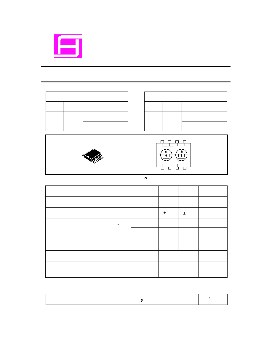
Dual E nhancement Mode Field E ffect Transistor ( N and P Channel)
P reliminary May.26 2004
ABS OLUTE MAXIMUM R ATINGS (T
A
=25 C unless otherwise noted)
Parameter
S ymbol
N-Channel P-Channel
Unit
Drain-S ource Voltage
V
DS
V
Gate-S ource Voltage
V
GS
V
Drain Current-Continuous @ T
J
=125 C
-Pulsed
I
D
2.0
A
A
A
W
I
DM
Drain-S ource Diode Forward Current
I
S
Maximum Power Dissipation
P
D
Operating Junction and S torage
Temperature R ange
T
J
, T
S TG
-55 to 150
C
THE R MAL CHAR ACTE R IS TICS
Thermal R esistance, Junction-to-Ambient
62.5
/W
C
a
a
a
a
b
30
1.7
-30
- 5
-1.7
1
P R ODUC T S UMMAR Y
V
DS S
I
D
R
DS (ON) ( m
W
) Max
30V
6.2A
32 @ V
G S
= 10V
57 @ V
G S
= 4.5V
S O-8
1
1
2
3
4
8
7
6
5
S
1
G
1
S
2
G
2
D
1
D
1
D
2
D
2
(N-C hannel)
P R ODUC T S UMMAR Y
V
DS S
I
D
-30V
-5A
45 @ V
G S
= -10V
60 @ V
G S
= -4.5V
(P -C hannel)
S amHop Microelectronics C orp.
20
20
6.2
25
- 20
R
JA
S T M8402
R
DS (ON) ( m
W
) Max
S T M8402
=
Parameter
Symbol
Condition
Min Typ Max Unit
OFF CHAR ACTER ISTICS
Drain-Source Breakdown Voltage
BV
DSS
=
V
GS
0V, I
D
250uA
=
30
V
Zero Gate Voltage Drain Current
I
DSS
V
DS
24V, V
GS
0V
=
=
1
Gate-Body Leakage
I
GSS
V
GS
20V, V
DS
0V
=
=
100 nA
ON CHAR ACTER ISTICS
b
Gate Threshold Voltage
V
GS(th)
V
DS
V
GS
, I
D
= 250uA
=
1
2.5
V
Drain-Source On-State R esistance
R
DS(ON)
V
GS
10V, I
D
9A
V
GS
4.5V, I
D
7A
57
On-State Drain Current
I
D(ON)
V
DS
= 10V, V
GS
= 10V
A
S
Forward Transconductance
FS
g
V
DS
10V, I
D
5A
DYNAMIC CHAR ACTER ISTICS
c
Input Capacitance
C
ISS
C
R SS
C
OSS
Output Capacitance
R everse Transfer Capacitance
V
DS
=15V, V
GS
= 0V
f =1.0MH
Z
P
F
P
F
P
F
SWITCHING CHAR ACTER ISTICS
c
Turn-On Delay Time
R ise Time
Turn-Off Delay Time
t
D(ON)
t
r
t
D(OFF)
t
f
V
DD
= 15V,
I
D
= 1A,
V
GS
= 10V,
R
GEN
= 6
ns
ns
ns
ns
Total Gate Charge
Gate-Source Charge
Gate-Drain Charge
Q
g
Q
gs
Q
gd
V
DS
=15V, I
D
= 9A,
V
GS
=10V
nC
nC
nC
C
Fall Time
=
=
=
=
=
=
2
5
32
1.7
uA
m ohm
m ohm
N-Channel ELECTRICAL CHARACTERISTICS (T
A
25 C unless otherwise noted)
V
DS
=15V, I
D
=9A,V
GS
=10V
nC
V
DS
=15V, I
D
=9A,V
GS
=4.5V
8
27
52
521
83
61
12.7
6.5
16.8
9.6
13. 6
9.6
2.7
2.9
18

=
Parameter
Symbol
Condition
Min Typ Max Unit
OFF CHAR ACTER ISTICS
Drain-Source Breakdown Voltage
BV
DSS
=
V
GS
0V, I
D
-250uA
=
-30
V
Zero Gate Voltage Drain Current
I
DSS
V
DS
-24V, V
GS
0V
=
=
-1
Gate-Body Leakage
I
GSS
V
GS
20V, V
DS
0V
=
=
nA
Gate Threshold Voltage
V
GS(th)
V
DS
V
GS
, I
D
= -250uA
=
-1
-1.5 -2.5
V
Drain-Source On-State R esistance
R
DS(ON)
V
GS
-10V, I
D
-4.5A
45
V
GS
-4.5V, I
D
-3.6A
50
60
On-State Drain Current
I
D(ON)
V
DS
= -5V, V
GS
= -10V
A
S
Forward Transconductance
FS
g
V
DS
-5V, I
D
- 5A
DYNAMIC CHAR ACTER ISTICS
c
Input Capacitance
C
ISS
C
R SS
C
OSS
Output Capacitance
R everse Transfer Capacitance
V
DS
=-15V, V
GS
= 0V
f =1.0MH
Z
P
F
P
F
P
F
SWITCHING CHAR ACTER ISTICS
c
Turn-On Delay Time
R ise Time
Turn-Off Delay Time
t
D(ON)
t
r
t
D(OFF)
t
f
V
D
= -15V,
R
L
= 15
I
D
= -1A,
V
GEN
= -10V,
R
GEN
= 6
ns
ns
ns
ns
Total Gate Charge
Gate-Source Charge
Gate-Drain Charge
Q
g
Q
gs
Q
gd
V
DS
=-15V, I
D
= - 4.9A,
V
GS
=-10V
nC
nC
nC
C
Fall Time
=
=
=
=
=
=
3
ON CHAR ACTER ISTICS
b
35
100
m ohm
m ohm
P-Channel ELECTRICAL CHARACTERISTICS (T
A
25 C unless otherwise noted)
nC
V
DS
=-15V,I
D
=-4.9A,V
GS
=-10V
V
DS
=-15V,I
D
=-4.9A,V
GS
=-4.5V
626
166
72
11.8
14.3
76.8
37.2
17.6
8.9
3.6
3.2
5
-15
uA
S T M8402
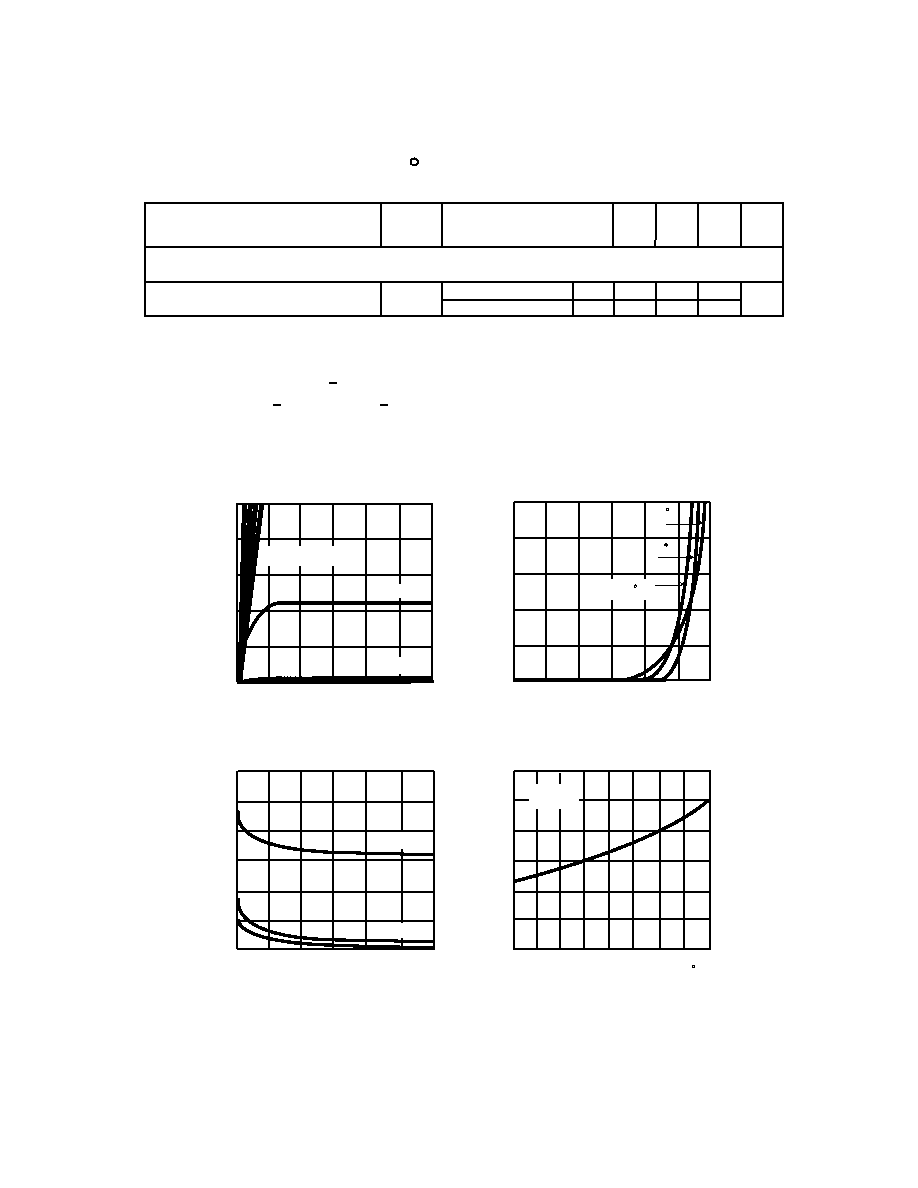
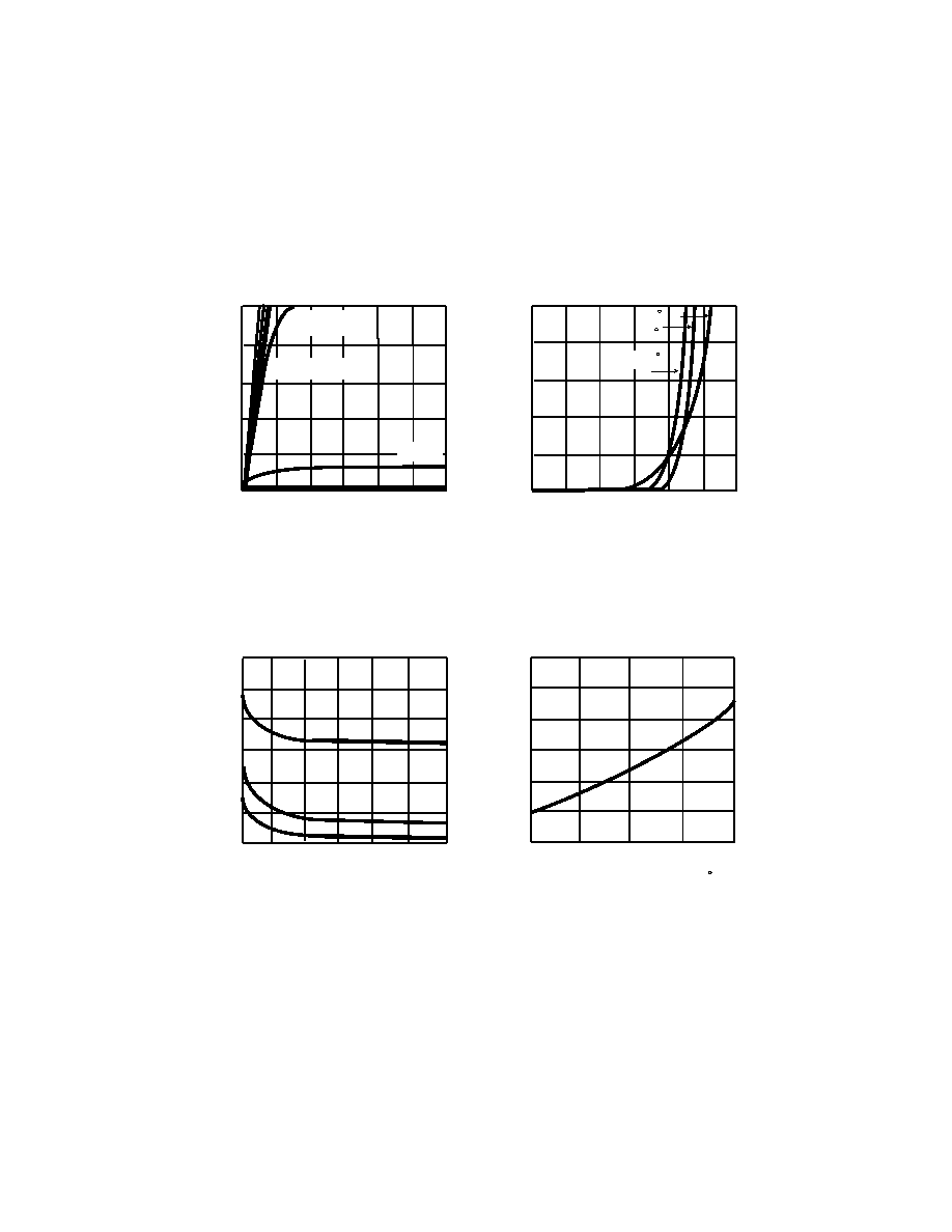
Figure 1. Output Characteristics
Figure 2. Transfer Characteristics
Figure 4. On-Resistance Variation with
Drain Current and Temperature
Figure 3. Capacitance
V
DS
, Drain-to Source Voltage (V)
V
GS
, Gate-to-Source Voltage (V)
V
DS
, Drain-to-Source Voltage (V)
I
D
, Drain Current(A)
I
D
,
D
r
a
i
n
C
u
r
r
e
n
t
(
A
)
C
,
C
a
p
a
c
i
t
a
n
c
e
(
p
F
)
O
n
-
R
e
s
i
s
t
a
n
c
e
(
O
h
m
s
)
I
D
,
D
r
a
i
n
C
u
r
r
e
n
t
(
A
)
4
R
D
S
(
O
N
)
,
5
10
8
6
4
2
0
0
1
2
3
4
5
6
V
GS
=10,9,8,7,6,5,4V
V
GS
=2.5V
-55 C
25 C
25
20
15
10
5
0
0.0
0.5
1.0
0.5
2.0
2.5
3.0
Tj=125 C
Tj( C )
1.6
1.4
1.2
1.0
0.6
0.4
0
0
50
100
150
1200
1000
800
600
400
200
0
0
5
10
15
20
25
30
Ciss
Coss
Crss
Parameter
Symbol
Condition
Min Typ Max Unit
ELECTRICAL CHARACTERISTICS (T
A
=25 C unless otherwise noted)
DRAIN-SOURCE DIODE CHARACTERISTICS
Diode Forward Voltage
V
SD
V
GS
= 0V, Is =1.7A
N-Ch
0.82
1.2
-0.8
-1.2
V
GS
= 0V, Is =-1.7A
P-Ch
V
b
C
Notes
c.Guaranteed by design, not subject to production testing.
b.Pulse Test:Pulse Width 300s, Duty Cycle 2%.
a.Surface Mounted on FR4 Board, t 10sec.
N-Channel
V
GS
=1.5V
-25
-50
25
75
125
V
G S
=10V
I
D
=9A
S T M8402
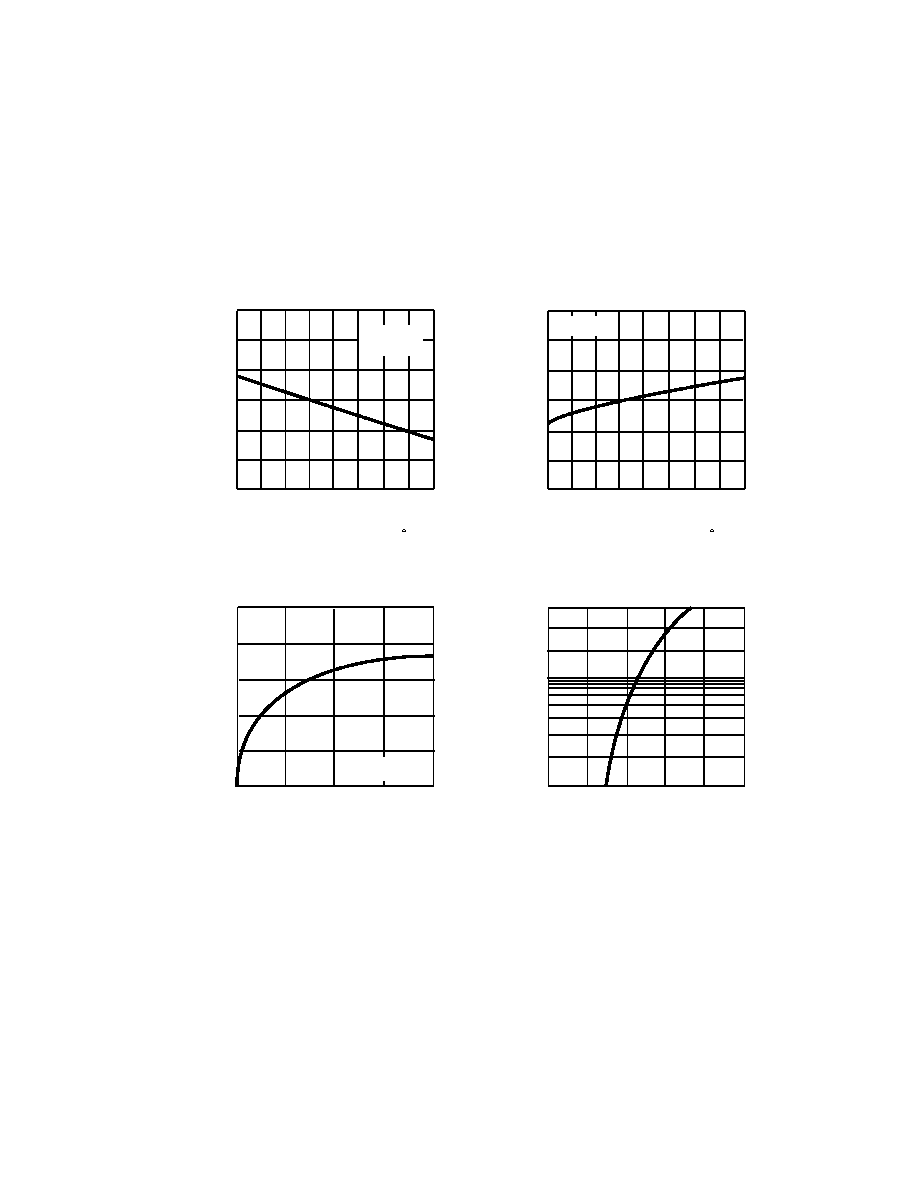
F igur e 5. G ate T hr eshold V ar iation
with T emper atur e
F igur e 6. B r eakdown V oltage V ar iation
with T emper atur e
V
t
h
,
N
o
r
m
a
l
i
z
e
d
G
a
t
e
-
S
o
u
r
c
e
T
h
r
e
s
h
o
l
d
V
o
l
t
a
g
e
g
F
S
,
T
r
a
n
s
c
o
n
d
u
c
t
a
n
c
e
(
S
)
B
V
D
S
S
,
N
o
r
m
a
l
i
z
e
d
D
r
a
i
n
-
S
o
u
r
c
e
B
r
e
a
k
d
o
w
n
V
o
l
t
a
g
e
I
s
,
S
o
u
r
c
e
-
d
r
a
i
n
c
u
r
r
e
n
t
(
A
)
with Dr ain C ur r ent
I
DS
, Drain-S ource C urrent (A)
F igur e 8. B ody Diode F or war d V oltage
V ar iation with Sour ce C ur r ent
V
S D
, B ody Diode F orward V oltage (V )
T j, J unction T emperature ( C )
T j, J unction T emperature ( C )
5
5
20.0
10.0
1.0
0.4
0.6
0.8
1.0
1.2
1.4
1.6
1.4
1.2
1.0
0.8
0.6
0.4
-50 -25
0
25
50
75 100 125 150
V
DS
=V
GS
I
D
=250
uA
-50 -25
0
25
50
75 100 125 150
1.15
1.10
1.05
1.00
0.95
0.90
0.85
I
D
=250
uA
12
9
6
3
15
0
0
5
10
15
20
V
DS
=10V
S T M8402
N-C hannel
F igur e 7. T r ansconductance V ar iation
S T M8402
6
P-C hannel
F igure 1. Output C har acter istics
F igure 2. Tr ansfer C har acter istics
F igure 3. C apacitance
-V
DS
, Drain-to S ource Voltage (V )
-V
G S
, G ate-to-S ource Voltage (V )
-V
DS
, Drain-to-S ource Voltage (V )
C
,
C
a
p
a
c
i
t
a
n
c
e
(
p
F
)
-
I
D
,
D
r
a
i
n
C
u
r
r
e
n
t
(
A
)
-
I
D
,
D
r
a
i
n
C
u
r
r
e
n
t
(
A
)
0 5 10 15 20 25 30
C iss
C oss
C rss
1200
1000
800
600
400
200
0
10
8
6
4
2
0
0
1
2
3
4
5
6
-V
G S
=2.5V
25 C
20
16
12
8
4
0
0
0.5
1
1.5
2
2.5
3
-55 C
T j=125 C
F igure 4. On-R esistance Var iation with
Temper ature
O
n
-
R
e
s
i
s
t
a
n
c
e
(
O
h
m
s
)
R
D
S
(
O
N
)
,
1.8
1.6
1.2
0.8
1.4
1.0
0.6
-50
0
50
100
150
V
G S
=-10V
T j, J unction T emperature ( C )
I
D
=-4.5A
(
N
o
r
m
a
l
i
z
e
d
)
-V
G S
=1.5V
-V
G S
=10,9,8,7,6,5,4V
F igur e 5. G ate T hr eshold V ar iation
with T emper atur e
F igur e 6. B r eakdown V oltage V ar iation
with T emper atur e
V
t
h
,
N
o
r
m
a
l
i
z
e
d
G
a
t
e
-
S
o
u
r
c
e
T
h
r
e
s
h
o
l
d
V
o
l
t
a
g
e
g
F
S
,
T
r
a
n
s
c
o
n
d
u
c
t
a
n
c
e
(
S
)
B
V
D
S
S
,
N
o
r
m
a
l
i
z
e
d
D
r
a
i
n
-
S
o
u
r
c
e
B
r
e
a
k
d
o
w
n
V
o
l
t
a
g
e
-
I
s
,
S
o
u
r
c
e
-
d
r
a
i
n
c
u
r
r
e
n
t
(
A
)
with Dr ain C ur r ent
-I
DS
, Drain-S ource C urrent (A)
F igur e 8. B ody Diode F or war d V oltage
V ar iation with Sour ce C ur r ent
-V
S D
, B ody Diode F orward V oltage (V )
T j, J unction T emperature ( C )
T j, J unction T emperature ( C )
7
5
20.0
10.0
1.0
0.4
0.6
0.8
1.0
1.2
1.4
1.6
1.4
1.2
1.0
0.8
0.6
0.4
-50 -25
0
25
50
75 100 125 150
V
DS
=V
GS
I
D
=-250
uA
-50 -25
0
25
50
75 100 125 150
1.15
1.10
1.05
1.00
0.95
0.90
0.85
I
D
=-250
uA
12
9
6
3
15
0
0
5
10
15
20
V
DS
=-10V
S T M8402
P-C hannel
F igur e 7. T r ansconductance V ar iation

S T M8402
8
5
N-C hannel
Q g, T otal G ate C harge (nC )
F igur e 9. G ate C har ge
F igur e 9. G ate C har ge
F igur e 10. M aximum Safe
O per ating A r ea
F igur e 10. M aximum Safe
O per ating A r ea
P-C hannel
-V
DS
, B ody Diode F orward V oltage (V )
Q g, T otal G ate C harge (nC )
V
DS
, Drain-S ource V oltage (V )
-
V
G
S
,
G
a
t
e
t
o
S
o
u
r
c
e
V
o
l
t
a
g
e
(
V
)
-
I
D
,
D
r
a
i
n
C
u
r
r
e
n
t
(
A
)
10
8
6
4
2
0
0
3
6
9
12
15 18
21 24
V
DS
=-15V
I
D
=-4.9A
50
10
1 1
0.1
0.03
0.1
1
10
50
R
DS
(O
N)
Li
mi
t
10m
s
100m
s
1s
DC
V
G S
=-10V
S ingle P ulse
T
A
=25 C
V
G
S
,
G
a
t
e
t
o
S
o
u
r
c
e
V
o
l
t
a
g
e
(
V
)
I
D
,
D
r
a
i
n
C
u
r
r
e
n
t
(
A
)
10
8
6
4
2
0
0
3
6
9
12
15 18 21 24
V
DS
=15V
I
D
=9A
40
10
1 1
0.1
0.03
0.1
1
10
30 50
10m
s
100m
s
1s
DC
V
G S
=10V
S ingle P ulse
T
A
=25 C
R
DS
(O
N)
Li
mi
t
F igur e 11. Switching T est C ir cuit
F igur e 12. Switching W avefor ms
t
V
V
t
t
d(on)
OUT
IN
on
r
10%
t
d(off)
90%
10%
10%
50%
50%
90%
t
off
t
f
90%
PULS E WIDTH
T
r
a
n
s
i
e
n
t
T
h
e
r
m
a
l
I
m
p
e
d
a
n
c
e
2
1
0.1
0.01
S quare Wave P ulse Duration (sec)
F igur e 13. Nor malized T her mal T r ansient I mpedance C ur ve
r
(
t
)
,
N
o
r
m
a
l
i
z
e
d
E
f
f
e
c
t
i
v
e
9
5
INVE R TE D
Duty C ycle=0.5
0.2
0.1
0.05
0.02
S ingle P ulse
10
-4
10
-3
10
-2
10
-1
1
10
100
P
DM
t
1
t
2
1. R
J A
(t)=r (t) * R
J A
2. R
J A
=S ee Datasheet
3. T
J M-
T
A
= P
DM
* R
J A
(t)
4. Duty C ycle, D=t
1
/t
2
V
DD
R
D
V
V
R
S
V
G
G S
IN
G E N
OUT
L
S T M8402
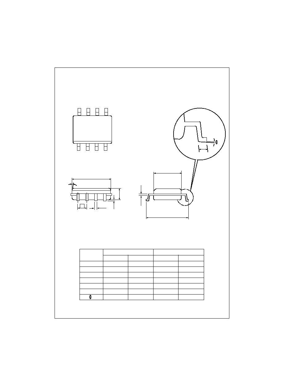
PAC K AG E OUT LINE DIME NS IONS
S O-8
10
S Y MB OLS
MIN
MIN
0.053
0.004
0.189
0.150
0.228
0.016
0∞
1.35
0.10
4.80
3.81
5.79
0.41
0∞
MAX
MAX
0.069
0.010
0.196
0.157
0.244
0.050
8∞
1.75
0.25
4.98
3.99
6.20
1.27
8∞
MILLIME T E R S
INC HE S
A
A1
D
E
H
L
1
e
B
H
E
L
A
1
A
C
D
0.05 TYP.
0.016 TYP.
0.008
TYP.
0.015X45∞
S T M8402
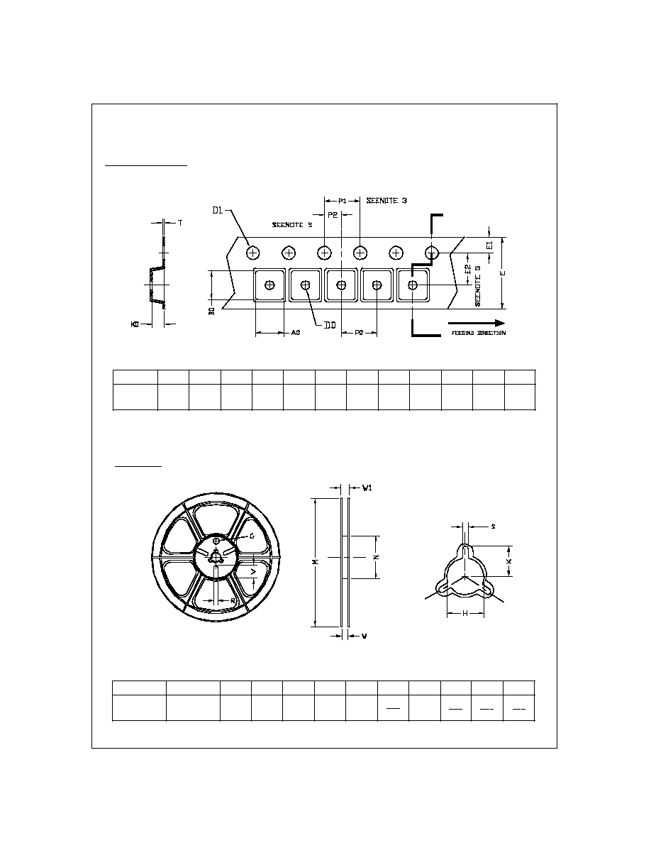
SO-8 Tape and Reel Data
SO-8 Carrier Tape
SO-8 Reel
unit:
PACKAGE
SOP 8N
150
A0
B0
K0
D0
D1
E
E1
E2
P0
P1
P2
T
6.40
5.20
2.10
1.5
(MIN)
1.5
+ 0.1
- 0.0
12.0
±
0.3
1.75
5.5
±
0.05
8.0
4.0
2.0
±
0.05
0.3
±
0.05
UNIT:
TAPE SIZE
12
REEL SIZE
330
M
N
W
W1
H
K
S
G
R
V
330
±
1
62
±
1.5
12.4
+ 0.2
16.8
- 0.4
12.75
+ 0.15
2.0
±
0.15
11
S T M8402