 | –≠–ª–µ–∫—Ç—Ä–æ–Ω–Ω—ã–π –∫–æ–º–ø–æ–Ω–µ–Ω—Ç: STM9410 | –°–∫–∞—á–∞—Ç—å:  PDF PDF  ZIP ZIP |
30
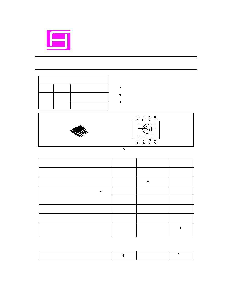
N-Channel Enhancement Mode Field Effect Transistor
Surface Mount Package.
ABSOLUTE MAXIMUM RATINGS (T
A
=25 C unless otherwise noted)
Parameter
Symbol
Limit
Unit
Drain-Source Voltage
V
DS
V
Gate-Source Voltage
V
GS
20
V
Drain Current-Continuous @T
A
=25 C
-Pulsed
I
D
6.3
25
1.7
2.5
A
A
A
W
I
DM
Drain-Source Diode Forward Current
I
S
Maximum Power Dissipation
P
D
Operating Junction and Storage
Temperature Range
T
J
, T
STG
-55 to 150
C
THERMAL CHARACTERISTICS
Thermal Resistance, Junction-to-Ambient
R
JA
50
/W
C
a
a
a
a
b
SamHop Microelectronics Corp.
PRODUCT SUMMARY
V
DSS
I
D
R
DS(ON) ( m
) MAX
30V
6.3A
32 @ V
GS
= 10V
55 @ V
GS
= 4.5V
FEATURES
Super high dense cell design for low R
DS(ON
).
Rugged and reliable.
SO-8
1
OCT.29, 2004 V1.1
1
STM9410
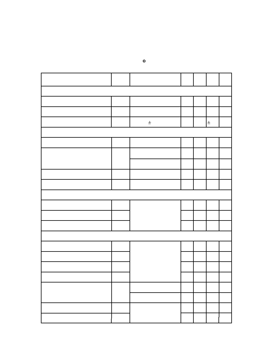
ELECTRICAL CHARACTERISTICS (T
A
25 C unless otherwise noted)
=
Parameter
Symbol
Condition
Min Typ Max Unit
OFF CHARACTERISTICS
Drain-Source Breakdown Voltage
BV
DSS
=
V
GS
0V, I
D
250uA
=
30
V
Zero Gate Voltage Drain Current
I
DSS
V
DS
24V, V
GS
0V
=
=
1
uA
Gate-Body Leakage
I
GSS
V
GS
20V, V
DS
0V
=
=
nA
ON CHARACTERISTICS
b
Gate Threshold Voltage
V
GS(th)
V
DS
V
GS
, I
D
= 250uA
=
1
V
Drain-Source On-State Resistance
R
DS(ON)
V
GS
10V, I
D
6A
32
V
GS
4.5V,I
D
5A
55
On-State Drain Current
I
D(ON)
V
DS
= 5V, V
GS
= 10V
A
S
Forward Transconductance
FS
g
V
DS
5V, I
D
6A
DYNAMIC CHARACTERISTICS
c
Input Capacitance
C
ISS
C
RSS
C
OSS
Output Capacitance
Reverse Transfer Capacitance
V
DS
=15V, V
GS
= 0V
f =1.0MH
Z
P
F
P
F
P
F
SWITCHING CHARACTERISTICS
c
Turn-On Delay Time
Rise Time
Turn-Off Delay Time
t
D(ON)
t
r
t
D(OFF)
t
f
V
DD
= 15V,
I
D
= 1A,
V
GS
= 10V,
R
GEN
= 10
ohm
ns
ns
ns
ns
Total Gate Charge
Gate-Source Charge
Gate-Drain Charge
Q
g
Q
gs
Q
gd
V
DS
=15V, I
D
= 1A,
V
GS
=10V
nC
nC
nC
C
Fall Time
=
=
=
=
=
=
2
100
m ohm
m ohm
nC
V
DS
=15V, I
D
=1A,V
GS
=10V
V
DS
=15V, I
D
=1A,V
GS
=4.5V
1.7
2.5
15
9
140
830
100
6
17
23
17
11
8
3
3
27
50
STM9410

Parameter
Symbol
Condition
Min Typ Max Unit
ELECTRICAL CHARACTERISTICS (T
A
=25 C unless otherwise noted)
DRAIN-SOURCE DIODE CHARACTERISTICS
Diode Forward Voltage
V
SD
V
GS
= 0V, Is =1.7A
0.82 1.1
V
b
C
Notes
c.Guaranteed by design, not subject to production testing.
b.Pulse Test:Pulse Width 300us, Duty Cycle 2%.
Figure 1. Output Characteristics
Figure 2. Transfer Characteristics
Figure 4. On-Resistance Variation with
Drain Current and Temperature
Figure 3. Capacitance
V
DS
, Drain-to Source Voltage (V)
V
GS
, Gate-to-Source Voltage (V)
V
DS
, Drain-to-Source Voltage (V)
I
D
, Drain Current(A)
I
D
,
D
r
a
i
n
C
u
r
r
e
n
t
(
A
)
C
,
C
a
p
a
c
i
t
a
n
c
e
(
p
F
)
O
n
-
R
e
s
i
s
t
a
n
c
e
(
O
h
m
s
)
I
D
,
D
r
a
i
n
C
u
r
r
e
n
t
(
A
)
a.Surface Mounted on FR4 Board, t 10sec.
3
R
D
S
(
O
N
)
,
10
8
6
4
2
0
0
0.5
1
1.5
2
2.5
3
V
GS
=5,4.3,2V
V
GS
=1.5V
-55 C
25 C
25
20
15
10
5
0
0.0
1.0
2.0
3.0
4.0
5.0
6.0
Tj=125 C
Tj=125 C
25 C
-55 C
0.030
0.025
0.020
0.015
0.010
0.005
0
0
5
10
15
20
V
GS
=10V
1200
1000
800
600
400
200
0
0
5
10
15
20
25
30
Ciss
Coss
Crss
STM9410

F igure 5. G ate T hres hold V ariation
with T emperature
F igure 6. B reakdown V oltage V ariation
with T emperature
V
t
h
,
N
o
r
m
a
l
i
z
e
d
G
a
t
e
-
S
o
u
r
c
e
T
h
r
e
s
h
o
l
d
V
o
l
t
a
g
e
g
F
S
,
T
r
a
n
s
c
o
n
d
u
c
t
a
n
c
e
(
S
)
V
G
S
,
G
a
t
e
t
o
S
o
u
r
c
e
V
o
l
t
a
g
e
(
V
)
B
V
D
S
S
,
N
o
r
m
a
l
i
z
e
d
D
r
a
i
n
-
S
o
u
r
c
e
B
r
e
a
k
d
o
w
n
V
o
l
t
a
g
e
I
s
,
S
o
u
r
c
e
-
d
r
a
i
n
c
u
r
r
e
n
t
(
A
)
F igure 7. T rans conductance V ariation
with Drain C urrent
I
DS
, Drain-S ource C urrent (A)
F igure 9. G ate C harge
Qg, T otal G ate C harge (nC )
F igure 10. Maximum S afe
O perating Area
V
DS
, Drain-S ource V oltage (V )
F igure 8. B ody Diode F orward V oltage
V ariation with S ource C urrent
V
S D
, B ody Diode F orward V oltage (V )
T j, J unction T emperature ( C )
T j, J unction T emperature ( C )
I
D
,
D
r
a
i
n
C
u
r
r
e
n
t
(
A
)
4
20.0
10.0
1.0
0.4
0.6
0.8
1.0
1.2
1.4
1.09
1.06
1.03
1.00
0.97
0.94
0.91
-50 -25
0
25
50
75 100 125 150
V
DS
=V
G S
I
D
=250uA
-50 -25
0
25
50
75 100 125 150
1.15
1.10
1.05
1.00
0.95
0.90
0.85
ID=-250uA
20
15
10
5
25
0
0
5
10
15
20
V
DS
=5V
40
10
1 1
0.1
0.03
0.1
1
10
30 50
R
DS
(O
N)
Li
mi
t
10m
s
100m
s
1s
DC
V
G S
=10V
S ingle P ulse
T
A
=25 C
10
8
6
4
2
0
0
3
6
9
12 15 18
21 24
V
DS
=15V
I
D
=1A
S T M9410
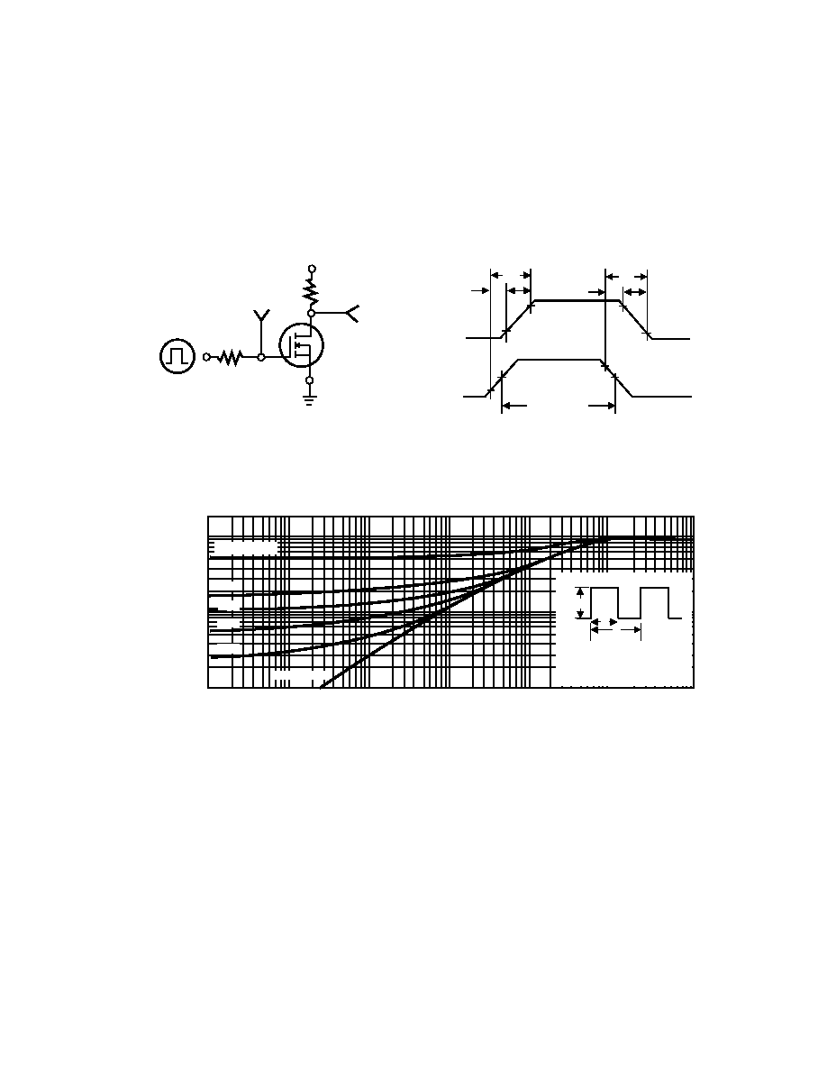
Figure 11. Switching Test Circuit
Figure 12. Switching Waveforms
V
DD
R
D
V
V
R
S
V
G
GS
IN
GEN
OUT
L
t
V
V
t
t
d(on)
OUT
IN
on
r
10%
t
d(off)
90%
10%
10%
50%
50%
90%
t
off
t
f
90%
PULSE WIDTH
T
r
a
n
s
i
e
n
t
T
h
e
r
m
a
l
I
m
p
e
d
a
n
c
e
2
1
0.1
0.01
Square Wave Pulse Duration (sec)
Figure 13. Normalized Thermal Transient Impedance Curve
r
(
t
)
,
N
o
r
m
a
l
i
z
e
d
E
f
f
e
c
t
i
v
e
5
INVERTED
Duty Cycle=0.5
0.2
0.1
0.05
0.02
Single Pulse
10
-4
10
-3
10
-2
10
-1
1
10
100
P
DM
t
1
t
2
1. R
qJA
(t)=r (t) * R
qJA
2. R
qJA
=See Datasheet
3. T
JM-
T
A
= P
DM
* R
qJA
(t)
4. Duty Cycle, D=t
1
/t
2
STM9410
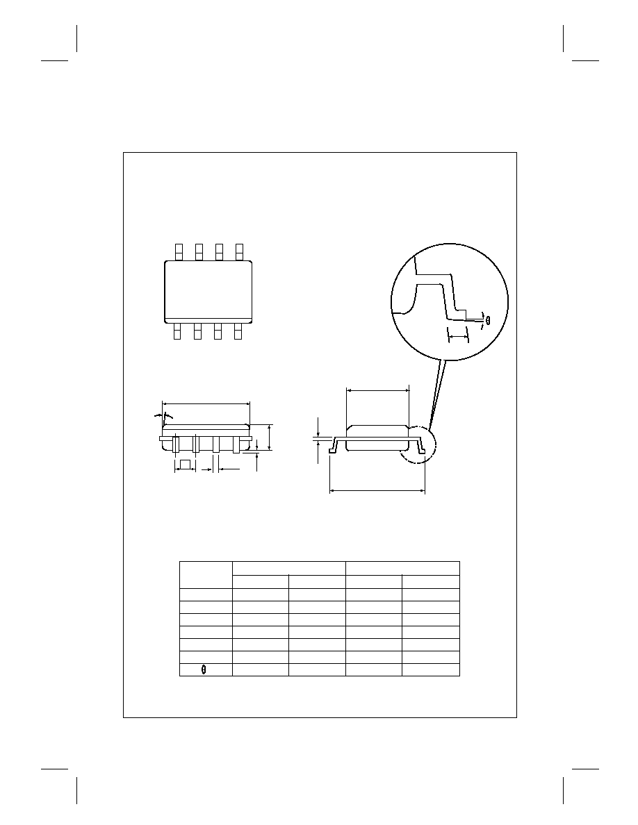
PACKAGE OUTLINE DIMENSIONS
SO-8
6
SYMBOLS
MIN
MIN
0.053
0.004
0.189
0.150
0.228
0.016
0∞
1.35
0.10
4.80
3.81
5.79
0.41
0∞
MAX
MAX
0.069
0.010
0.196
0.157
0.244
0.050
8∞
1.75
0.25
4.98
3.99
6.20
1.27
8∞
MILLIMETERS
INCHES
A
A1
D
E
H
L
1
e
B
H
E
L
A
1
A
C
D
0.05 TYP.
0.016 TYP.
0.008
TYP.
0.015X45∞
STM9410

SO-8 Tape and Reel Data
SO-8 Carrier Tape
SO-8 Reel
unit:
PACKAGE
SOP 8N
150
A0
B0
K0
D0
D1
E
E1
E2
P0
P1
P2
T
6.40
5.20
2.10
1.5
(MIN)
1.5
+ 0.1
- 0.0
12.0
±
0.3
1.75
5.5
±
0.05
8.0
4.0
2.0
±
0.05
0.3
±
0.05
UNIT:
TAPE SIZE
12
REEL SIZE
330
M
N
W
W1
H
K
S
G
R
V
330
±
1
62
±
1.5
12.4
+ 0.2
16.8
- 0.4
12.75
+ 0.15
2.0
±
0.15
7
STM9410