 | –≠–ª–µ–∫—Ç—Ä–æ–Ω–Ω—ã–π –∫–æ–º–ø–æ–Ω–µ–Ω—Ç: STS2321 | –°–∫–∞—á–∞—Ç—å:  PDF PDF  ZIP ZIP |

-20
P-Channel Enhancement Mode Field Effect Transistor
Oct .29 2004 V1.1
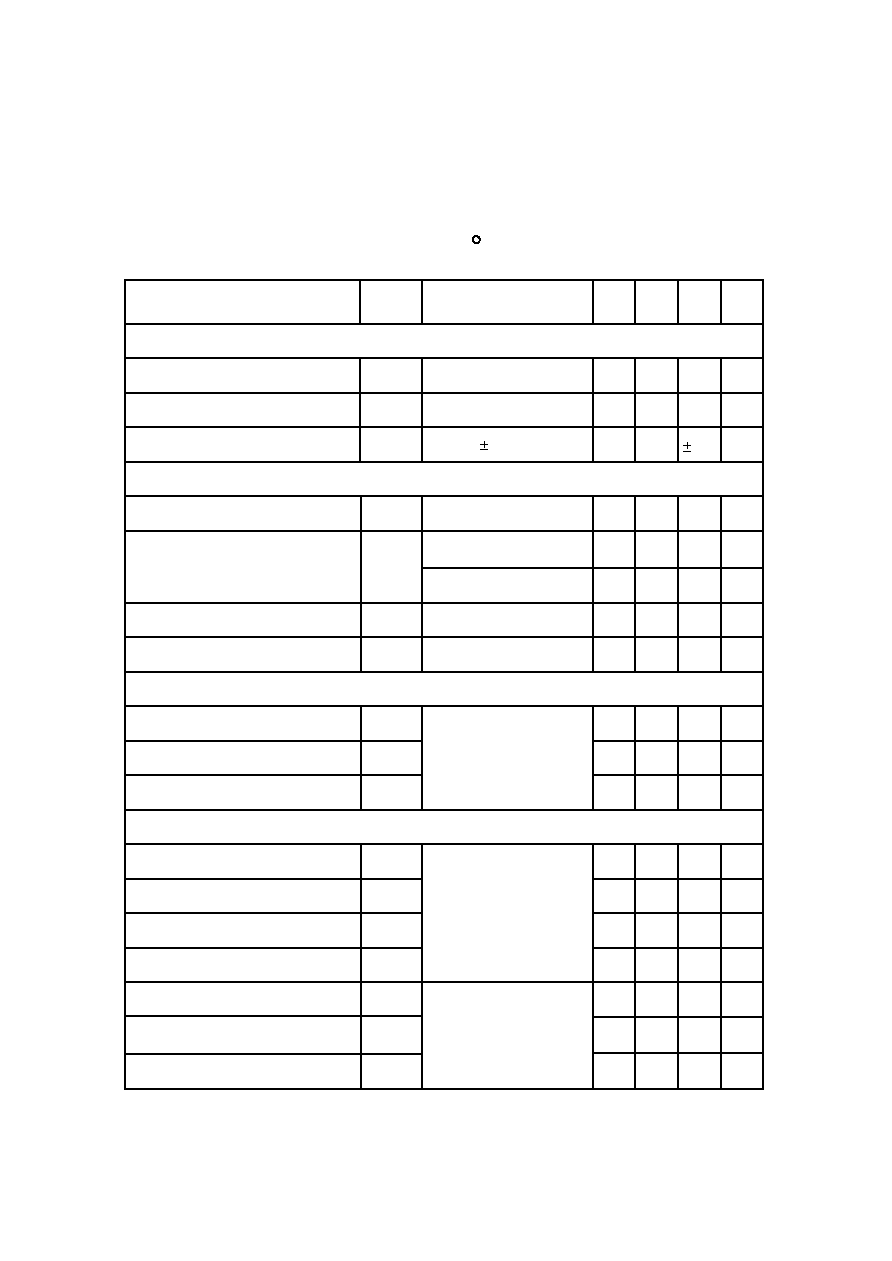
ABSOLUTE MAXIMUM RATINGS (T
A
=25 C unless otherwise noted)
Parameter
Symbol
Limit
Unit
Drain-Source Voltage
V
DS
V
Gate-Source Voltage
V
GS
V
Drain Current-Continuous @T
J
=25 C
-Pulsed
I
D
-3.2
A
A
A
W
I
DM
-11
Drain-Source Diode Forward Current
I
S
-1.25
Maximum Power Dissipation
P
D
Operating Junction and Storage
Temperature Range
T
J
, T
STG
-55 to 150
C
THERMAL CHARACTERISTICS
Thermal Resistance, Junction-to-Ambient
R
thJA
100
/W
C
STS2321
1.25
a
a
a
a
b
G
D
S
SOT-23
S
G
D
1
SamHop Microelectronics Corp.
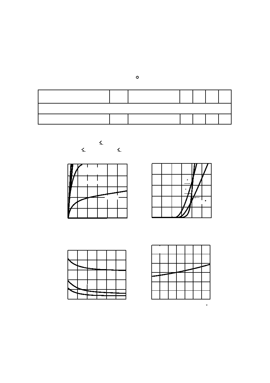
PRODUCT SUMMARY
V
DSS
I
D
R
DS(ON) ( m
W
) Max
-20V
-3.2A
65 @ V
GS
= -4.5V
90 @ V
GS
=-2.5V
FEATURES
Super high dense cell design for low R
DS(ON
).
Rugged and reliable.
SOT-23 package.
10
ELECTRICAL CHARACTERISTICS (T
A
25 C unless otherwise noted)
=
Parameter
Symbol
Condition
Min Typ Max Unit
OFF CHARACTERISTICS
Drain-Source Breakdown Voltage
BV
DSS
=
V
GS
0V, I
D
-250uA
=
-20
V
Zero Gate Voltage Drain Current
I
DSS
V
DS
-16V, V
GS
0V
=
=
1
uA
Gate-Body Leakage
I
GSS
V
GS
10V, V
DS
0V
=
=
100 nA
ON CHARACTERISTICS
b
Gate Threshold Voltage
V
GS(th)
V
DS
V
GS
, I
D
=-250uA
=
-0.6
-1.5
V
Drain-Source On-State Resistance
R
DS(ON)
V
GS
-4.5V, I
D
-3.2A
50
65
V
GS
-2.5V, I
D
-2.0A
75
90
On-State Drain Current
I
D(ON)
V
DS
= -5V, V
GS
= -4.5V
A
S
Forward Transconductance
FS
g
V
DS
-5V, I
D
DYNAMIC CHARACTERISTICS
c
Input Capacitance
C
ISS
C
RSS
C
OSS
Output Capacitance
Reverse Transfer Capacitance
V
DS
= -15V, V
GS
= 0V
f =1.0MH
Z
P
F
P
F
P
F
SWITCHING CHARACTERISTICS
c
Turn-On Delay Time
Rise Time
Turn-Off Delay Time
t
D(ON)
t
r
t
D(OFF)
t
f
V
DD
= -10V,
I
D
= -1A,
V
GS
= -4.5V,
R
L
= 10
ohm
R
GEN
= 6
ohm
ns
ns
ns
ns
Total Gate Charge
Gate-Source Charge
Gate-Drain Charge
Q
g
Q
gs
Q
gd
V
DS
= -10V, I
D
= -3.2A,
V
GS
= -4.5V
nC
nC
nC
C
Fall Time
=
=
=
=
=
2
m-ohm
m-ohm
8
= -3.2A
8
610
155
105
13.9
7.1
75.2
54
7.4
1.2
2.8
-0.9
STS2321
STS2321
Parameter
Symbol
Condition
Min Typ Max Unit
ELECTRICAL CHARACTERISTICS (T
A
=25 C unless otherwise noted)
DRAIN-SOURCE DIODE CHARACTERISTICS
Diode Forward Voltage
V
SD
V
GS
= 0V, Is =-1.25A
-0.78 -1.2
V
b
C
Notes
c.Guaranteed by design, not subject to production testing.
b.Pulse Test:Pulse Width 300us, Duty Cycle 2%.
Figure 1. Output Characteristics
Figure 2. Transfer Characteristics
Figure 4. On-Resistance Variation with
Temperature
Figure 3. Capacitance
-V
DS
, Drain-to Source Voltage (V)
-V
GS
, Gate-to-Source Voltage (V)
-V
DS
, Drain-to-Source Voltage (V)
-
I
D
,
D
r
a
i
n
C
u
r
r
e
n
t
(
A
)
C
,
C
a
p
a
c
i
t
a
n
c
e
(
p
F
)
O
n
-
R
e
s
i
s
t
a
n
c
e
(
N
o
r
m
a
l
i
z
e
d
)
-
I
D
,
D
r
a
i
n
C
u
r
r
e
n
t
(
A
)
a.Surface Mounted on FR4 Board, t 10sec.
R
D
S
(
O
N
)
,
5
0 5 10 15 20 25 30
Ciss
Coss
1000
800
600
400
200
0
20
16
12
8
4
0
0
2
4
6
8
10
12
-V
GS
=10,9,8,7,6,5,4V
3
2.2
1.8
1.4
1.0
0.6
0.2
0
-50
0
50
100 125
Tj( C)
-25
25
75
V
GS
=-4.5V
I
D
=-3.2A
Crss
25 C
25
20
15
10
5
0
0.0
0.2
0.4
0.6
0.8
1.0
Tj=125 C
-55 C
-V
GS
=2V
-V
GS
=3V
1.2
with Temperature
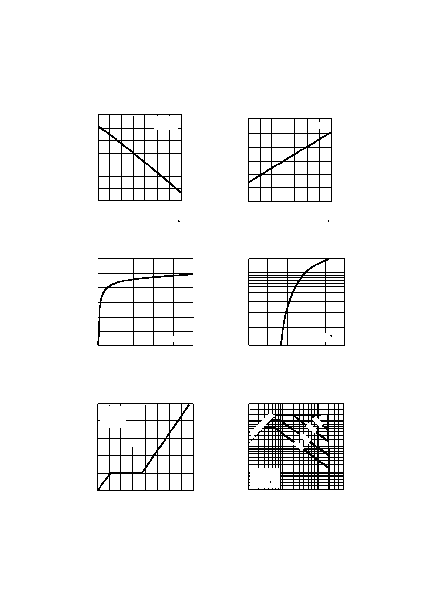
Figure 6. Breakdown Voltage Variation
with Temperature
V
t
h
,
N
o
r
m
a
l
i
z
e
d
G
a
t
e
-
S
o
u
r
c
e
T
h
r
e
s
h
o
l
d
V
o
l
t
a
g
e
g
F
S
,
T
r
a
n
s
c
o
n
d
u
c
t
a
n
c
e
(
S
)
-
V
G
S
,
G
a
t
e
t
o
S
o
u
r
c
e
V
o
l
t
a
g
e
(
V
)
B
V
D
S
S
,
N
o
r
m
a
l
i
z
e
d
D
r
a
i
n
-
S
o
u
r
c
e
B
r
e
a
k
d
o
w
n
V
o
l
t
a
g
e
-
I
s
,
S
o
u
r
c
e
-
d
r
a
i
n
c
u
r
r
e
n
t
(
A
)
Figure 7. Transconductance Variation
with Drain Current
-I
DS
, Drain-Source Current (A)
Figure 9. Gate Charge
Qg, Total Gate Charge (nC)
Figure 10. Maximum Safe
Operating Area
-V
DS
, Drain-Source Voltage (V)
Figure 8. Body Diode Forward Voltage
Variation with Source Current
-V
SD
, Body Diode Forward Voltage (V)
Tj, Junction Temperature ( C)
Tj, Junction Temperature ( C)
-
I
D
,
D
r
a
i
n
C
u
r
r
e
n
t
(
A
)
20
10
0
1
0.4
0.6
0.8
1.0
1.2
1.4
4
3
2
1
0
0
1 2 3
4
5
6
7
8
V
DS
=-10V
I
D
=-3.2A
T
J
=25 C
13
10
1 1
0.1
0.03
0.1
1
10 20
50
R
DS
(O
N)
Li
mi
t
10m
s
100
ms
1s
DC
V
GS
=-4.5V
Single Pulse
Tc=25 C
4
-50 -25
0
25 50
75 100 125
1.10
1.07
1.04
1.00
0.97
0.94
0.91
I
D
=-250uA
1.3
1.2
1.1
1.0
0.9
0.8
0.7
0.6
-50 -25
0
25 50
75 100 125
V
DS
=V
GS
I
D
=-250uA
10
8
6
4
12
0
0
5
10
15
20
25
2
V
DS
=-5V
5
STS2321
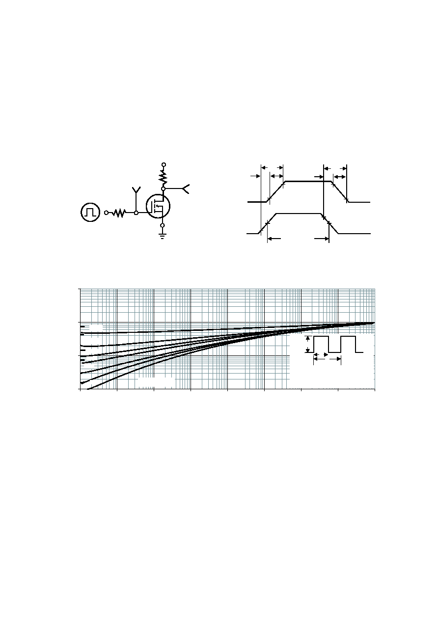
Figure 11. Switching Test Circuit
Figure 12. Switching Waveforms
t
V
V
t
t
d(on)
OUT
IN
on
r
10%
t
d(off)
90%
10%
10%
50%
50%
90%
t
off
t
f
90%
PULSE WIDTH
5
INVERTED
V
DD
R
D
V
V
R
S
V
G
GS
IN
GEN
OUT
L
5
0.01
0.1
1
10
0.00001
0.0001
0.001
0.01
0.1
1
10
100
1000
Square Wave Pulse Duration(sec)
Normalized Thermal Transient Impedance Curve
N
o
r
m
a
l
i
z
e
d
T
r
a
n
s
i
e
n
t
T
h
e
r
m
a
l
R
e
s
i
s
t
a
n
c
e
Single Pulse
on
P
DM
t
1
t
2
1. R
thJA
(t)=r (t) * R
JA
2. R
JA
=See Datasheet
3. T
JM-
T
A
= P
DM
* R
JA
(t)
4. Duty Cycle, D=t
1
/t
2
th
th
th
0.01
0.02
0.5
0.2
0.1
0.05
STS2321
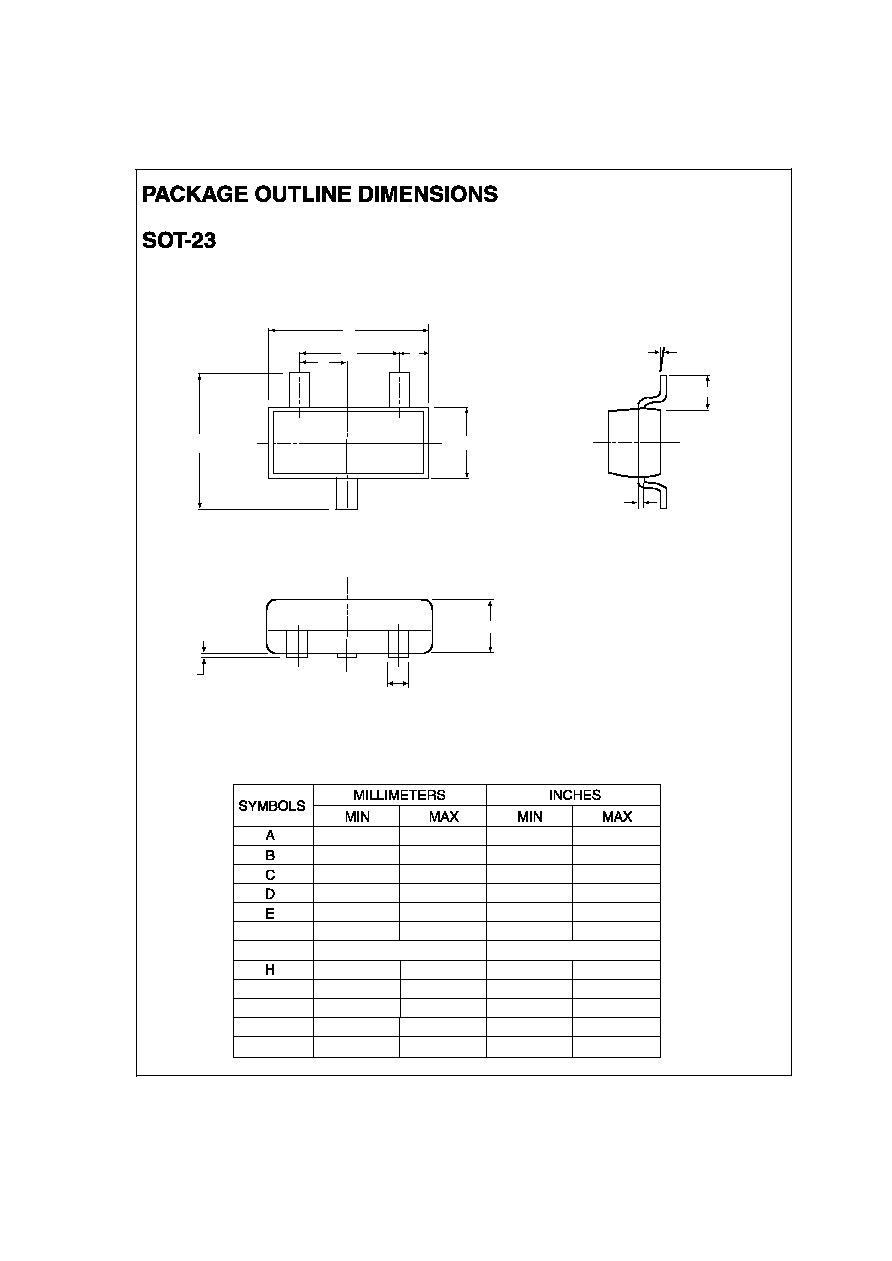
J
2.70
2.40
1.40
0.35
0
0.45
1.90 REF.
1.00
0.10
3.10
2.80
1.60
0.50
0.10
0.55
1.30
0.20
0.106
0.094
0.055
0.014
0
0.018
0.039
0.004
0.122
0.110
0.063
0.020
0.004
0.022
0.051
0.008
0.40
0.45
1.15
0.016
0.033
0.045
6
G
A
F
C
B
L
D (TYP.)
E
H
M
I
F
G
I
J
L
M
0.075 REF.
-
-
0∞
10∞
0∞
10∞
STS2321
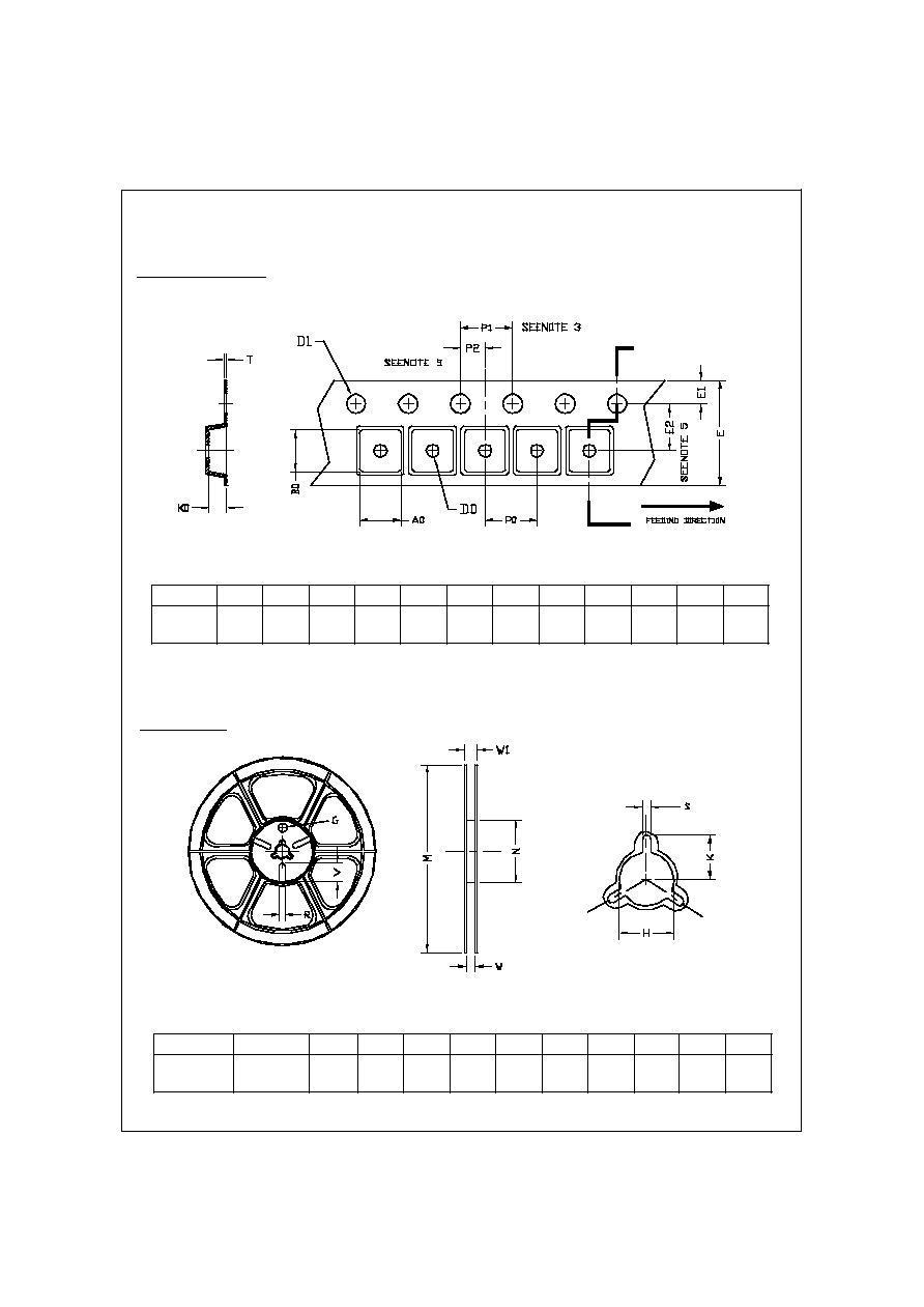
SOT-23 Tape and Reel Data
SOT-23 Carrier Tape
SOT-23 Reel
7
3.20
±0.10
3.00
±0.10
1.33
±0.10
1.00
+0.25
1.50
+0.10
8.00
+0.30
-0.10
1.75
±0.10
3.50
±0.05
4.00
±0.10
4.00
±0.10
2.00
±
0.05
0.20
±
0.02
178
178
±1
60
±1
9.00
±
0.5
12.00
±
0.5
13.5
±
0.5
2.00
±
0.5
10.0
18.00
5.00
8
V
UNIT:
R
G
S
K
H
W1
W
N
M
10.5
REEL SIZE
TAPE SIZE
UNIT:
PACKAGE
SOT-23
A0
B0
K0
D0
D1
E
E1
E2
P0
P1
P2
T
STS2321