20
AB S OLUTE MAXIMUM R ATING (T
A
=25 C unles s otherwis e noted)
Parameter
S ymbol
Limit
Unit
Drain-S ource Voltage
V
DS
V
Gate-S ource Voltage
V
GS
V
Drain Current-Continuous @ T
c
=25 C
-Pulsed
I
D
2.5
A
A
A
W
I
DM
8
Drain-S ource Diode Forward Current
I
S
1.25
Maximum Power Dissipation
P
D
Operating Junction and S torage
Temperature R ange
T
J
, T
S TG
-55 to 150
C
THE R MAL CHAR ACTE R IS TICS
Thermal R esistance, Junction-to-Ambient
R
thJA
125
/W
C
1
a
a
a
a
b
1
S amHop Microelectronics C orp.
P R ODUC T S UMMAR Y
V
DS S
I
D
R
DS (ON) ( m
W
) Max
20V
2.5A
80 @ V
G S
= 4.5V
F E AT UR E S
S uper high dense cell design for low R
DS (ON
).
R ugged and reliable.
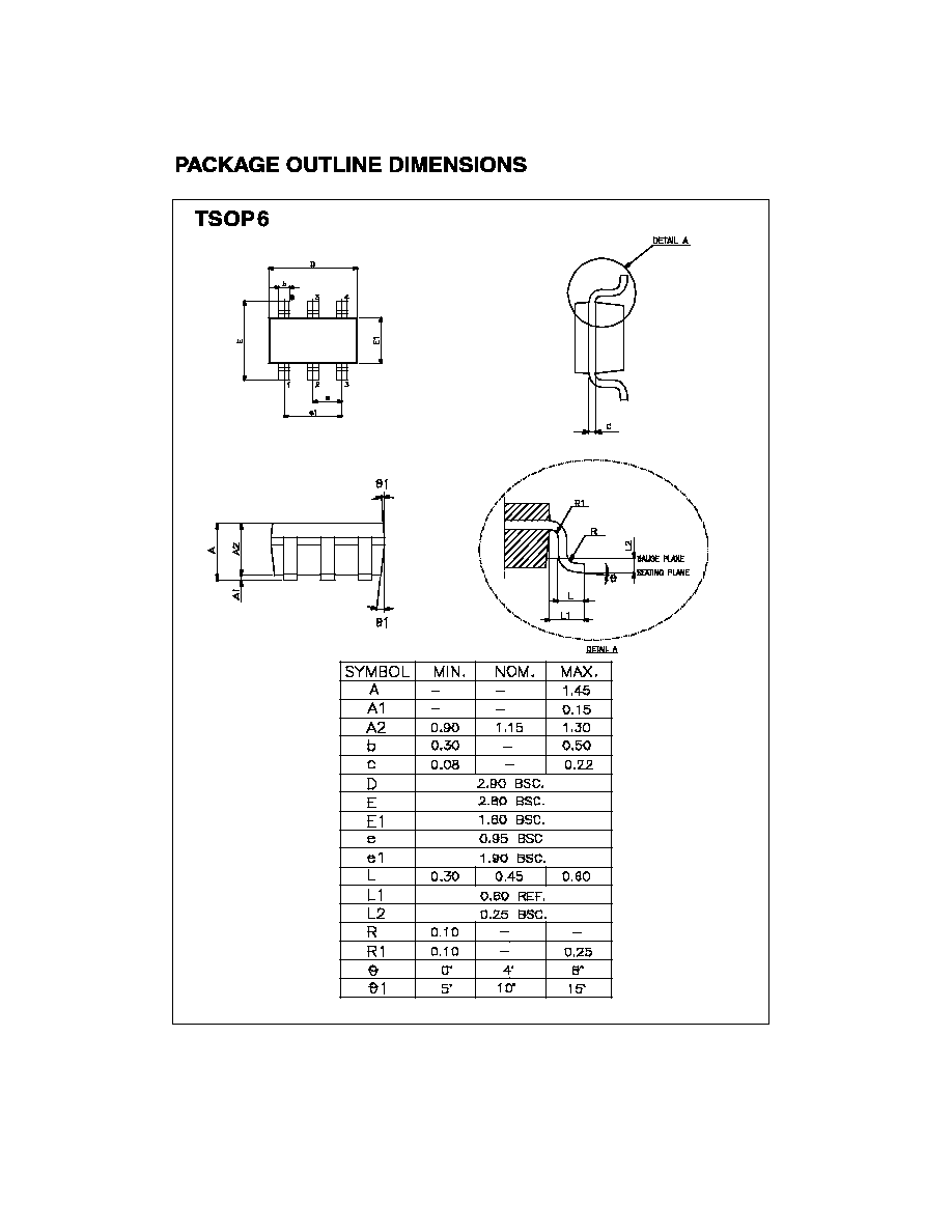
TS OP6 package.
10
110 @ V
G S
= 2.5V
S T S 2622
F eb,25 2005 V er1.1
G2
S 1
G1
D1
D2
S 2
TS OP6
Top View
S 1
D2
S 2
G1
D1
G2
1
2
3
6
5
4
Dual N-Channel E nhancement Mode Field E ffect Transistor
E LE CTR ICAL CHAR ACTE R IS TICS (T
A
25 C unless otherwise noted)
=
Parameter
Symbol
Condition
Min Typ Max Unit
OFF CHAR ACTER ISTICS
Drain-Source Breakdown Voltage
BV
DSS
=
V
GS
0V, I
D
250uA
=
20
V
Zero Gate Voltage Drain Current
I
DSS
V
DS
16V, V
GS
0V
=
=
1
uA
Gate-Body Leakage
I
GSS
V
GS
10V, V
DS
0V
=
=
100 nA
ON CHAR ACTER ISTICS
b
Gate Threshold Voltage
V
GS(th)
V
DS
V
GS
, I
D
= 250uA
=
0.5
1.5
V
Drain-Source On-State R esistance
R
DS(ON)
V
GS
4.5V, I
D
2A
80
V
GS
2.5V, I
D
1A
On-State Drain Current
I
D(ON)
V
DS
= 5V, V
GS
= 4.5V
A
S
Forward Transconductance
FS
g
V
DS
5V, I
D
DYNAMIC CHAR ACTER ISTICS
c
Input Capacitance
C
ISS
C
R SS
C
OSS
Output Capacitance
R everse Transfer Capacitance
V
DS
=10V, V
GS
= 0V
f =1.0MH
Z
P
F
P
F
P
F
SWITCHING CHAR ACTER ISTICS
c
Turn-On Delay Time
R ise Time
Turn-Off Delay Time
t
D(ON)
t
r
t
D(OFF)
t
f
V
DD
= 10V,
I
D
= 1A,
V
GS
= 4.5V,
R
GEN
= 6
ohm
ns
ns
ns
ns
Total Gate Charge
Gate-Source Charge
Gate-Drain Charge
Q
g
Q
gs
Q
gd
V
DS
=10V, I
D
= 2.5A,
V
GS
=4.5V
nC
nC
nC
C
Fall Time
=
=
=
=
=
2
m-ohm
m-ohm
=2.5A
110
6
7
S T S 2622
220
67
50
10.2
8.3
13.5
12.7
4
1.5
0.7
0.8
65
90
S T S 2622
Parameter
S ymbol
Condition
Min Typ Max Unit
E LE CTR ICAL CHAR ACTE R IS TICS (T
A
=25 C unless otherwise noted)
DR AIN-S OUR CE DIODE CHAR ACTE R IS TICS
Diode Forward Voltage
V
S D
V
GS
= 0V, Is =1.25A
0.84 1.2
V
b
C
Notes
c.Guaranteed by design, not subject to production testing.
b.Pulse Test:Pulse Width 300us, Duty Cycle 2%.
F igure 1. Output C haracteristics
F igure 2. Transfer C haracteristics
F igure 4. On-R esistance Variation with
Temperature
F igure 3. C apacitance
V
DS
, Drain-to S ource Voltage (V )
V
G S
, G ate-to-S ource Voltage (V )
V
DS
, Drain-to-S ource Voltage (V )
I
D
,
D
r
a
i
n
C
u
r
r
e
n
t
(
A
)
C
,
C
a
p
a
c
i
t
a
n
c
e
(
p
F
)
I
D
,
D
r
a
i
n
C
u
r
r
e
n
t
(
A
)
a.Surface Mounted on FR 4 Board, t 10sec.
5
0 5 10 15 20 25 30
C iss
C oss
500
400
300
200
100
0
20
16
12
8
4
0
0
0.5
1
1.5
2
2.5
3
V
G S
=4V
V
G S
=2V
3
2.2
1.8
1.4
1.0
0.6
0.2
0
-50
0
50
100
125
T j( C )
-25
25
75
V
G S
=4.5V
I
D
=2.5A
C rss
25 C
15
12
9
6
3
0
0.0
0.6
1.2
1.8
2.4
3.0
3.6
T j=125 C
-55 C
V
G S
=3V
V
G S
=4.5V
V
G S
=10V
O
n
-
R
e
s
i
s
t
a
n
c
e
R
D
S
(
O
N
)
,
N
o
r
m
a
l
i
z
e
d
with T emperature
F igure 6. B reakdown V oltage V ariation
with T emperature
V
t
h
,
N
o
r
m
a
l
i
z
e
d
G
a
t
e
-
S
o
u
r
c
e
T
h
r
e
s
h
o
l
d
V
o
l
t
a
g
e
g
F
S
,
T
r
a
n
s
c
o
n
d
u
c
t
a
n
c
e
(
S
)
V
G
S
,
G
a
t
e
t
o
S
o
u
r
c
e
V
o
l
t
a
g
e
(
V
)
B
V
D
S
S
,
N
o
r
m
a
l
i
z
e
d
D
r
a
i
n
-
S
o
u
r
c
e
B
r
e
a
k
d
o
w
n
V
o
l
t
a
g
e
I
s
,
S
o
u
r
c
e
-
d
r
a
i
n
c
u
r
r
e
n
t
(
A
)
F igure 7. T rans conductance V ariation
with Drain C urrent
I
DS
, Drain-S ource C urrent (A)
F igure 9. G ate C harge
Qg, T otal G ate C harge (nC )
F igure 10. Maximum S afe
O perating Area
V
DS
, Drain-S ource V oltage (V )
F igure 8. B ody Diode F orward V oltage
V ariation with S ource C urrent
V
S D
, B ody Diode F orward V oltage (V )
T j, J unction T emperature ( C )
T j, J unction T emperature ( C )
I
D
,
D
r
a
i
n
C
u
r
r
e
n
t
(
A
)
20
10
0
1
0.4
0.8
1.2
1.6
2.0
2.4
4
5
3
2
1
0
0
0.7 1.4 2.1 2.8 3.5 4.2 4.9 5.6
V
DS
=4.5V
I
D
=2.5A
T
J
=25 C
50
10
1 1
0.1
0.03
0.1
1
10 20
50
R
DS
(O
N)
Li
mi
t
10m
s
100
ms
1s
DC
V
G S
=4.5V
S ingle P ulse
Tc=25 C
4
-50 -25
0
25
50
75 100 125
1.3
1.2
1.1
1.0
0.9
0.8
0.7
I
D
=250uA
1.3
1.2
1.1
1.0
0.9
0.8
0.7
0.6
-50 -25
0
25
50
75 100 125
V
DS
=V
G S
I
D
=250uA
S T S 2622
10
8
6
4
12
0
0
3
6
9
12
15
2
V
DS
=5V
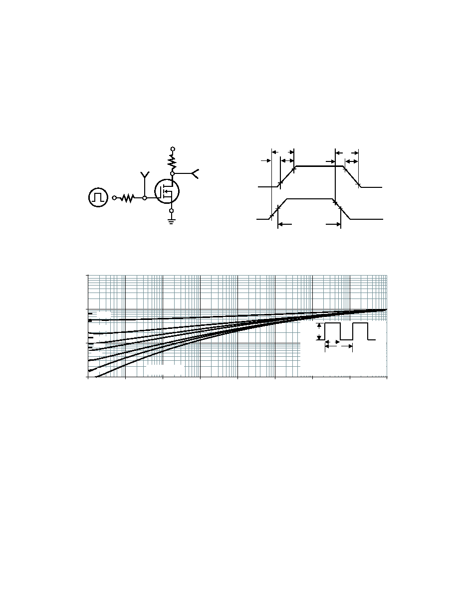
F igure 11. S witching T est C ircuit
F igure 12. S witching Waveforms
t
V
V
t
t
d(on)
OUT
IN
on
r
10%
t
d(off)
90%
10%
10%
50%
50%
90%
t
off
t
f
90%
PULS E WIDTH
5
INVE R TE D
V
DD
R
D
V
V
R
S
V
G
G S
IN
G E N
OUT
L
5
S T S 2622
0.01
0.1
1
10
0.00001
0.0001
0.001
0.01
0.1
1
10
100
1000
Square Wave Pulse Duration(sec)
Normalized Thermal Transient Impedance Curve
N
o
r
m
a
l
i
z
e
d
T
r
a
n
s
i
e
n
t
T
h
e
r
m
a
l
R
e
s
i
s
t
a
n
c
e
Single Pulse
on
P
DM
t
1
t
2
1. R
thJ A
(t)=r (t) * R
J A
2. R
J A
=S ee Datasheet
3. T
J M-
T
A
= P
DM
* R
J A
(t)
4. Duty C ycle, D=t
1
/t
2
th
th
th
0.01
0.02
0.5
0.2
0.1
0.05
6
S T S 2622
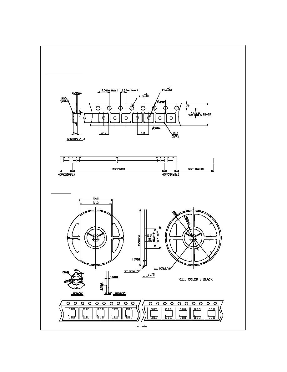
TSOP6 Tape and Reel Data
TSOP6 Carrier Tape
TSOP6 Reel
7
S T S 2622