ADC1275X
0.18
µ
µ
m 12-BIT 500KSPS ADC
1
GENERAL DESCRIPTION
The ADC1275X is a CMOS 3.3V 12-bit analog-to- digital converter (ADC). It converts the analog input signal into 12-
bit binary digital codes at a maximum conversion rate of 500KSPS with 2.5MHz clock. The device is a recycling type
monolithic ADC with an on-chip sample-and-hold function. The ADC has power down mode.
FEATURES
-- Resolution : 12-bit
-- Maximum Conversion Rate : 500KSPS
-- Main Clock : 2.5MHz
-- Power Supply : 3.3V
±
0.3V
-- Total Current : 1uA (Standby Mode)
1.8mA (Normal Operation)
-- Input Range : 0.0V ≠ 3.3V (3.3V
P-P
)
-- Differential Linearity
Error :
±
1.0 LSB (Max)
-- Integral Linearity Error :
±
3.0 LSB (Max.)
-- Signal to Noise & Distortion Ratio : 62dB
-- Digital Output : CMOS Level
-- Operating Temperature Range : -40
∞
C ≠ 85
∞
C
TYPICAL APPLICATIONS
-- Micom Interface
-- Portable Equipment
-- Low-Voltage Low-Power Application

0.18
µ
µ
m 12-BIT 500KSPS ADC
ADC1275X
2
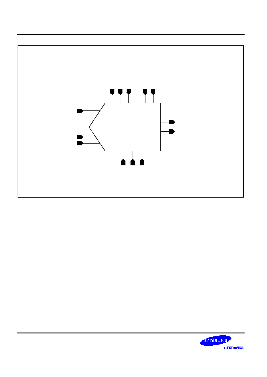
FUNCTIONAL BLOCK DIAGRAM
AINT
VREF
AGND
DO[11:0]
EOC
STC
CKIN
STBY
MAIN
BIAS
REF
GEN
CML
GEN
CLOCK
GEN
MDAC1
FLASH1
MDAC2
FLASH2
DIGITAL
LOGIC
Ver 1.4 (Mar. 2003)
No responsibility is assumed by SEC for its use nor for any infringements of patents or other rights of third parties
that may result from its use. The content of this data sheet is subject to change without any notice.
ADC1275X
0.18
µ
µ
m 12-BIT 500KSPS ADC
3
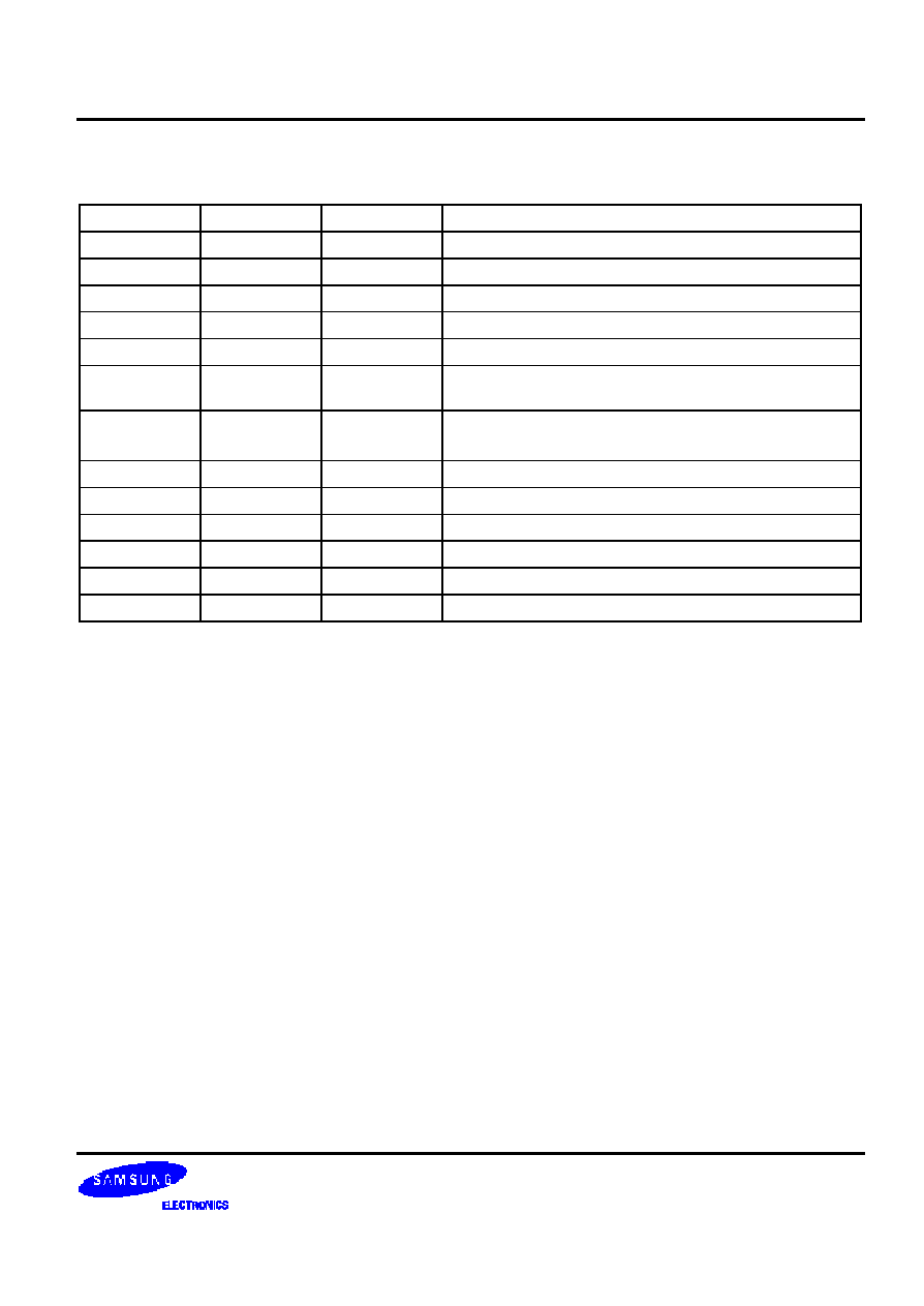
CORE PIN DESCRIPTION
Name
I/O Type
I/O Pad
Pin Description
VREF
AI
phia_abb
Reference Top (3.3V)
AGND
AI
phia_abb
Reference Bottom (0.0V)
AVDD33A1
AP
vdd3t_abb
Analog Power (3.3V)
AVBB33A1
AG
vbb3_abb
Analog Sub Bias (0.0V)
AVSS33A1
AG
vss3t_abb
Analog Ground (0.0V)
AINT
AI
phiar50_abb
Analog Input
(Input Range : 0.0V ~ 3.3V)
STBY
DI
phicc_abb
V
DD
=power saving (standby),
GND=normal
CKIN
DI
phicc_abb
Sampling Clock Input
D[11:0]
DO
phot4_abb
Digital Output
EOC
DO
phot4_abb
End of Conversion Signal
STC
DI
phicc_bb
Start of Conversion Signal
AVSS33A2
DG
vss3t_abb
Digital GND (0.0V)
AVDD33A2
DP
vdd3t_abb
Digital Power (3.3V)
I/O Type Abbr.
-- AI: Analog Input
-- DI: Digital Input
-- AO: Analog Output
-- DO: Digital Output
-- AP: Analog Power
-- AG: Analog Ground
-- DP: Digital Power
-- DG: Digital Ground
-- AB: Analog Bi-direction
-- DB: Digital Bi-direction

ADC1275X
0.18
µ
µ
m 12-BIT 500KSPS ADC
5
ABSOLUTE MAXIMUM RATINGS
Characteristic
Symbol
Value
Unit
Supply Voltage
V
DD
3.8
V
Analog Input Voltage
AINT
V
SS
to V
DD
V
Digital Input Voltage
CKIN
V
SS
to V
DD
V
Reference Voltage
VREF/AGND
V
SS
to V
DD
V
Storage Temperature Range
Tstg
-45 to 150
∞
C
Operating Temperature Range
Topr
-40 to 85
∞
C
NOTES:
1. Absolute maximum rating specifies the values beyond which the device may be damaged permanently. Exposure to
ABSOLUTE MAXIMUM RATING conditions for extended periods may affect reliability. Each condition value is applied
with the other values kept within the following operating conditions and function operation under any of these conditions
is not implied.
2. All voltages are measured with respect to V
SS
unless otherwise specified.
3. 100pF capacitor is discharged through a 1.5k
resistor (Human body model)
RECOMMENDED OPERATING CONDITIONS
Characteristics
Symbol
Min
Typ
Max
Unit
Supply Voltage
AVDD33A1
AVDD33A2
3.0
3.3
3.6
V
Reference Input Voltage
VREF
AGND
2.0
0.0
3.3
0.0
3.6
0.0
V
Analog Input Voltage
AINT
0.0
VREF
≠
V
Operating Temperature
Toper
-40
≠
85
∞
C
NOTE: It is strongly recommended that all the supply pins (AVDD33A1, AVDD33A2) be powered from the same source to
avoid power latch-up.
DC ELECTRICAL CHARACTERISTICS
Characteristics
Symbol
Min
Typ
Max
Unit
Test Conditions
Differential Nonlinearity
DNL
≠
±
0.8
±
1
LSB
VREF=3.3V
AGND=0.0V
Integral Nonlinearity
INL
≠
±
1.8
±
3
LSB
VREF=3.3V
AGND=0.0V
Offset Voltage
OFF
≠
10
16
LSB
VREF=3.3V
AGND=0.0V
(Converter Specifications : AVDD33A1=AVDD33A2=3.3V, AVSS33A1=AVSS33A2=0V, Toper=25
∞
C, VREF=3.3V,
AGND=0.0V unless otherwise specified)