 | –≠–ª–µ–∫—Ç—Ä–æ–Ω–Ω—ã–π –∫–æ–º–ø–æ–Ω–µ–Ω—Ç: adc1341x | –°–∫–∞—á–∞—Ç—å:  PDF PDF  ZIP ZIP |

ADC1341X
0.13
µ
µ
m 10-BIT 500KSPS ADC
1
GENERAL DESCRIPTION
The adc1341x_pc is a CMOS 3.3V 10-bit analog-to-digital converter (ADC). It converts the analog input signal
into 10-bit binary digital codes at a maximum conversion rate of 500KSPS with 2.5MHz clock.
The device is a recycling type monolithic ADC with an on-chip sample-and-hold function. The ADC has power
down mode.
FEATURES
-- Resolution: 10-bit
-- Maximum conversion rate: 500KSPS
-- Main clock: 2.5MHz (max.)
-- Power supply: 3.3V
±
0.3V
-- Total current: 20uA (Standby Mode)
2.5mA (Normal Operation)
-- Input range: 0.0V ~ 3.3V (3.3V
P-P
)
-- Differential linearity error:
±
1.0 LSB
-- Integral linearity error:
±
2.0 LSB
-- Signal to noise & distortion ratio: 54dB (Typ.)
-- Digital output: CMOS Level
-- Operating temperature range: ≠40
∞
C ~ 85
∞
C
TYPICAL APPLICATIONS
-- MICOM interface
-- Portable equipment
-- Low-voltage low-power application
0.13
µ
µ
m 10-BIT 500KSPS ADC
ADC1341X
2
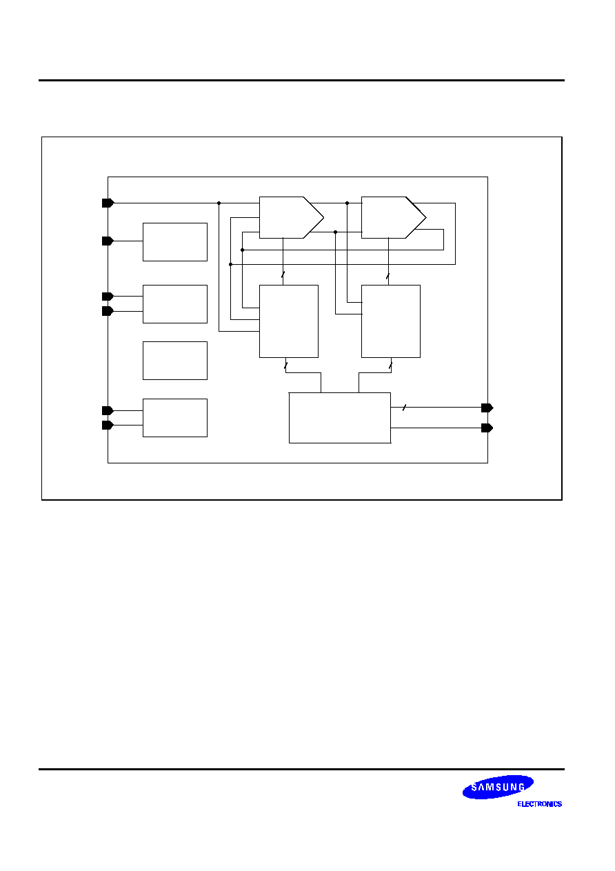
FUNCTIONAL BLOCK DIAGRAM
CLOCK
GEN
AINT
VREF
AGND
DO[9:0]
STC
CKIN
STBY
CML
GEN
REF
GEN
MAIN
BIAS
FLASH2
FLASH1
Digital Logic
EOC
MDAC1
MDAC2
Ver 1.0 (Apr. 2002)
This data sheet is a preliminary version. No responsibility is assumed by SEC for its use nor for any infringements of patents
or other rights of third parties that may result from its use. The content of this data sheet is subject to change without any
notice.
ADC1341X
0.13
µ
µ
m 10-BIT 500KSPS ADC
3
CORE PIN DESCRIPTION
Name
I/O Type
I/O Pad
Pin Description
VREF
AI
phia_abb
Reference top (3.3V)
AGND
AI
phia_abb
Reference bottom (0.0V)
AVDD33A1
AP
vdd3th_abb
Analog power (3.3V)
AVBB33A1
AG
vbbh_abb
Analog sub bias (0.0V)
AVSS33A1
AG
vssth_abb
Analog ground (0.0V)
AINT
AI
phiar50_abb
Analog input (input range: 0.0V ~ 3.3V)
STBY
DI
phicc_abb
VDD = Power saving (standby),
GND = Normal
CKIN
DI
phicc_abb
Sampling clock input
D[9:0]
DO
phob4_abb
Digital output
EOC
DO
phob4_abb
End of conversion signal
STC
DI
phicc_bb
Start of conversion signal
AVSS33A2
DG
vssth_abb
Digital GND (0.0V)
AVDD33A2
DP
vdd3th_abb
Digital power (3.3V)
I/O
Type
Abbr.
-- AI: Analog Input
-- DI: Digital Input
-- AO: Analog Output
-- DO: Analog Output
-- AP: Analog Power
-- AG: Analog Ground
-- DP: Digital Power
-- DG: Digital Ground
-- AB: Analog Bi-Direction
-- DB: Digital Bi-Direction

0.13
µ
µ
m 10-BIT 500KSPS ADC
ADC1341X
4
CORE CONFIGURATION
STBY
CKIN
AINT
VREF
AGND
AVDD33A1
AVSS33A1
AVBB33A1
AVDD33A2
AVSS33A2
[MSB:LSB]
STC
DO[9:0]
EOC
adc1341x

ADC1341X
0.13
µ
µ
m 10-BIT 500KSPS ADC
5
ABSOLUTE MAXIMUM RATINGS
Characteristics
Symbol
Value
Unit
Supply voltage
VDD
3.8
V
Analog input voltage
AINT
VSS to VDD
V
Digital input voltage
CKIN
VSS to VDD
V
Reference voltage
VREF / AGND
VSS to VDD
V
Storage temperature range
Tstg
≠45 to 150
∞
C
Operating temperature range
Topr
≠40 to 85
∞
C
NOTES:
1.
Absolute
maximum
rating
specifies
the
values
beyond
which
the
device
may
be
damaged
permanently.
Exposure
to
absolute
maximum
rating
conditions
for
extended
periods
may
affect
reliability.
Each
condition
value
is
applied
with
the
other
values
kept
within
the
following
operating
conditions
and
function
operation
under
any
of
these
conditions
is
not
implied.
2.
All
voltages
are
measured
with
respect
to
VSS
unless
otherwise
specified.
3.
100pF
capacitor
is
discharged
through
a
1.5k
resistor
(Human
body
model)
RECOMMENDED OPERATING
CONDITIONS
Characteristics
Symbol
Min
Typ
Max
Unit
Supply voltage
AVDD33A1
AVDD33A2
3.0
3.3
3.6
V
Reference input voltage
VREF
AGND
2.0
0.0
3.3
0.0
3.6
0.0
V
Analog input voltage
AINT
0.0
VREF
≠
V
Operating temperature
Toper
≠40
≠
85
∞
C
NOTE: It is strongly recommended that all the supply pins (AVDD33A1, AVDD33A2) be powered from the same source to
avoid power latch-up.
DC ELECTRICAL
CHARACTERISTICS
Characteristics
Symbol
Min
Typ
Max
Unit
Test Condition
Differential nonlinearity
DNL
≠
±
0.8
±
1
LSB
VREF = 3.3V
AGND = 0.0V
Integral nonlinearity
INL
≠
±
1
±
2
LSB
VREF = 3.3V
AGND = 0.0V
Offset voltage
OFF
≠
3
8
LSB
VREF = 3.3V
AGND = 0.0V
(Converter
Specifications:
AVDD33A1=AVDD33A2=3.3V,
AVSS33A1=AVSS33A2=0V,
Toper=25
∞
C,
VREF=3.3V,
AGND=0.0V
unless
otherwise
specified)
0.13
µ
µ
m 10-BIT 500KSPS ADC
ADC1341X
6
AC ELECTRICAL
CHARACTERISTICS
Characteristics
Symbol
Min
Typ
Max
Unit
Test Condition
Maximum conversion rate
fc
≠
≠
500
KSPS
f
CKIN
= 2.5MHz
Standby supply current
≠
≠
20
40
uA
STBY = VDD
Dynamic supply current
IVDD
≠
2.3
3
mA
f
CKIN
= 2.5MHz
(without system load)
Reference current
IREF
≠
0.4
0.6
mA
V
REF
= 3.3V
Total harmonic distortion
THD
≠
-60
≠56
dB
f
CKIN
= 2.5MHz
AINT = 100kHz
Signal-to-noise & distortion
ratio
SNDR
50
54
≠
dB
f
CKIN
= 2.5MHz
AINT = 100kHz
(Converter
Specifications:
AVDD33A1=AVDD33A2=3.3V,
AVSS33A1=AVSS33A2=0V,
Toper=25
∞
C,
VREF=3.3V,
AGND=0.0V
unless
otherwise
specified)
I/O
CHART
Index
AINT Input (V)
Digital Output
0
~ 0.00322
00 0000 0000
1LSB = 3.22mV
1
0.00322 ~ 0.00644
00 0000 0001
VREF = 3.3V
2
0.00644 ~ 0.00967
00 0000 0010
AGND = 0.0V
~
~
~
511
1.64678 ~ 1.65000
01 1111 1111
512
1.65000 ~ 1.65322
10 0000 0000
513
1.65322 ~ 1.65644
10 0000 0001
~
~
~
1021
3.29033 ~ 3.29355
11 1111 1101
1022
3.29355 ~ 3.29678
11 1111 1110
1023
3.29678 ~
11 1111 1111

ADC1341X
0.13
µ
µ
m 10-BIT 500KSPS ADC
7
TIMING DIAGRAM
1. Main Waveform
STBY
STC
DO[9:0]
CKIN
Input Sampling Period
AINT
EOC
A2
1
2
3
4
5
A1
2. STC & CKIN Condition
10ns
CKIN
STC
3ns
T
SAFE
The A/D Converter operates data conversion when STC (Start Conversion) signal is just "HIGH". Otherwise,
output data (DO[9:0]) keep the current states. The STC signal should be changed during "T
SAFE
" with the "HIGH"
level of the clock to operation as shown in the main waveform.
∑
ADC External Interface Signal
AINT: Analog Input Signal (Input)
Input Range: VREF ~ AGND
STBY: Stand-by Signal, Power Save Mode (Input)
CKIN: ADC Main Clock, f
CKIN
= 2.5MHz, 1 Clock Period = 400ns (Input)
STC: Start of Conversion Signal (Input)
EOC: End of Conversion Signal (Output)
DO[9:0]: Digital Output Signal (Output)
0.13
µ
µ
m 10-BIT 500KSPS ADC
ADC1341X
8
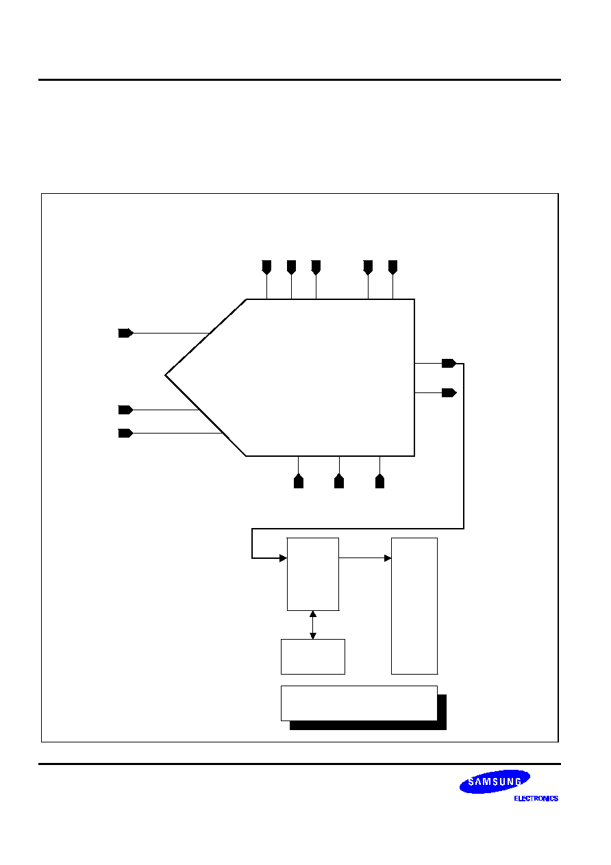
CORE EVALUATION GUIDE
ADC function is evaluated by external check on the bi-directional pads connected to input nodes of HOST DSP
back-end circuit.
The reference voltages may be biased internally through resistor divider.
STBY
CKIN
AINT
VREF
AGND
AVDD33A1
AVSS33A1
AVBB33A1
AVDD33A2
AVSS33A2
[MSB:LSB]
STC
DO[9:0]
EOC
Digital
Mux
HOST
DSP
CORE
Bi-directional
PAD
D[9:0]
D[9:0]
D[9:0]
(ADC Function Test & Externally
Forced Digital Input)
adc1341x

ADC1341X
0.13
µ
µ
m 10-BIT 500KSPS ADC
9
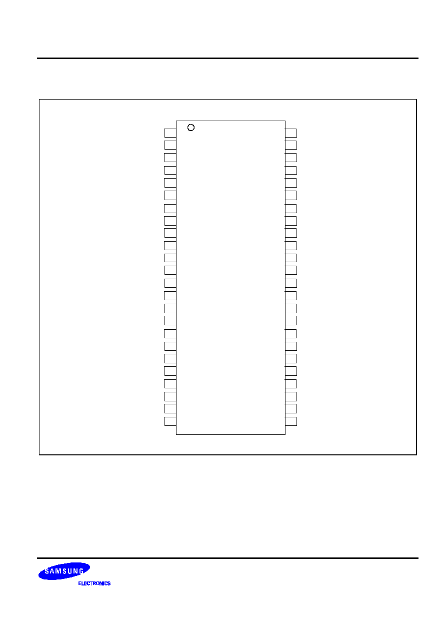
PACKAGE CONFIGURATION
adc1341x
48
47
VREF
VREF
AGND
AGND
NC
AVDD33A1
AVDD33A1
AVBB33A1
AVSS33A1
AVSS33A1
AINT
NC
NC
NC
NC
NC
STBY
VDDR
VSSR
CKIN
NC
NC
NC
RP
AVDD33A2
AVDD33A2
AVSS33A2
AVDD33A2
NC
STC
EOC
NC
NC
DO[9]
DO[8]
DO[7]
DO[6]
DO[5]
DO[4]
DO[3]
DO[2]
DO[1]
DO[0]
NC
RN
10u
0.1u
10u
Digital I
Digital II
Analog
NC
NC
NC
46
45
44
43
42
41
40
39
38
37
36
35
34
33
32
31
30
29
28
27
26
25
1
2
3
4
5
6
7
8
9
10
11
12
13
14
15
16
17
18
19
20
21
22
23
24
0.1u
10u
0.1u
0.1u
10u
10u 0.1u
10u 0.1u
NOTE: NC denotes "No Connection".

0.13
µ
µ
m 10-BIT 500KSPS ADC
ADC1341X
10
PACKAGE PIN DESCRIPTION
Name
No.
I/O Type
Pin Description
VREF
1, 2
AI
Reference voltage (3.3V)
AGND
3, 4
AI
Analog ground (0.0V)
AVDD33A1
6, 7
AP
Analog power (3.3V)
AVBB33A1
8
AG
Analog sub bias
AVSS33A1
9, 10
AG
Analog ground
AINT
11
AI
Analog input
STBY
17
DI
VDD = Power saving (Standby), GND = Normal
VDDR
18
PP
PAD power (3.3V)
VSSR
19
PG
PAD ground
CKIN
20
DI
Clock input (f
CKIN
= 2.5MHz)
RP
24
AO
Test pin1
RN
25
AO
Test pin2
DO[0]
29
DO
Digital output (LSB)
DO[1:8]
30 ~ 37
DO
Digital output
DO[9]
38
DO
Digital output (MSB)
EOC
41
DO
End of conversion signal
STC
42
DI
Start of conversion signal
AVSS33A2
45, 46
DG
Digital GND
AVSS33A2
47, 48
DP
Digital power (3.3V)
ADC1341X
0.13
µ
µ
m 10-BIT 500KSPS ADC
11
PACKAGE CONFIGURATION
VREF
VBBA
NC
NC
NC
RN
adc1341x
VREF
AGND
NC
VDDA
VDDA
VSSA
VSSA
AINT
NC
NC
NC
NC
NC
STBY
VDDR
VSSR
CKIN
VDDD
VDDD
VSSD
VSSD
NC
STC
EOC
NC
NC
DO[9]
DO[8]
DO[7]
DO[6]
DO[5]
DO[4]
DO[3]
DO[2]
DO[1]
DO[0]
NC
RP
AGND
NC
NC
NC
48
47
46
45
44
43
42
41
40
39
38
37
36
35
34
33
32
31
30
29
28
27
26
25
1
2
3
4
5
6
7
8
9
10
11
12
13
14
15
16
17
18
19
20
21
22
23
24
NOTE: I/O TYPE PP and PG denote PAD Power and PAD Ground respectively.

0.13
µ
µ
m 10-BIT 500KSPS ADC
ADC1341X
12
USER GUIDE
INPUT RANGE
The analog input is single-ended type and the range is from VREF to AGND. This AINT voltage follows reference
voltage range fundamentally. So, if you want to alter into the another input range, you should change the voltage
value of VREF.
You can use the AINT voltage whose minimum range is 2.0V. In this case, the VREF is 2.0V.
PHANTOM CELL INFORMATION
DO[8]
DO[0]
DO[4]
DO[2]
DO[3]
DO[5]
DO[6]
DO[7]
DO[1]
STC
CKIN
EOC
AVDD33A2
AVBB33A1
AVSS33A2
STBY
VREF
AGND
AVSS33A1
AVBB33A1
AVDD33A1
adc1341x
DO[9]
AINT

ADC1341X
0.13
µ
µ
m 10-BIT 500KSPS ADC
13
Name
I/O Type
Pin Usage
Pin Description
AINT
AI
Internal/External
AINT signal should not be crossed by any signals and
should not run next to digital signals to minimize
capacitive coupling between the two signals.
STBY
DI
Internal/External
Digital input signal lines must have same length to
reduce propagation delay.
CKIN
DI
Internal/External
D[9:0]
DO
Internal/External
EOC
DO
Internal/External
STC
DI
Internal/External
VREF
AI
External
Voltage reference lines (VREF and AGND) must be wide
metal to reduce voltage drop of metal lines.
AGND
AI
External
AVDD33A1
AP
External
It is recommended that you use thick analog power
metal. When connected to PAD, the path should be
kept as short as possible.
AVBB33A1
AG
External
Digital power and analog power are separately used.
AVSS33A1
AG
External
AVSS33A2
DG
External
AVDD33A2
DP
External

0.13
µ
µ
m 10-BIT 500KSPS ADC
ADC1341X
14
FEEDBACK
REQUEST
It should be quite helpful to our ADC core development if you specify your system requirements on ADC in the
following characteristic checking table and fill out the additional questions.
We appreciate your interest in our products. Thank you very much.
Parameter
Min
Typ
Max
Unit
Remarks
Analog power supply voltage
V
Digital power supply voltage
V
Bit resolution
Bit
Reference input voltage
V
Analog input voltage
Vpp
Operating temperature
∞
C
Integral non-linearity error
LSB
Differential non-linearity error
LSB
Bottom offset voltage error
mV
Top offset voltage error
mV
Maximum conversion rate
MSPS
Dynamic supply current
mA
Power dissipation
mW
Signal-to-noise ratio
dB
Digital output format (provide detailed
description & timing diagram)
-- Between single input-output and differential input-output configurations, which one is suitable for your system
and why?
-- Please comment on the internal/external pin configurations you want our ADC to have, if you have any
reason to prefer some type of configuration.
-- Freely list those functions you want to be implemented in our ADC, if you have any.
ADC1341X
0.13
µ
µ
m 10-BIT 500KSPS ADC
15
HISTORY CARD
Version
Date
Modified Items
Comments
Ver1.0
02. 04
Original version published (preliminary)