 | –≠–ª–µ–∫—Ç—Ä–æ–Ω–Ω—ã–π –∫–æ–º–ø–æ–Ω–µ–Ω—Ç: adc1394x | –°–∫–∞—á–∞—Ç—å:  PDF PDF  ZIP ZIP |

ADC1394X
0.13
µ
µ
m 8-BIT 20MSPS ADC
1
GENERAL DESCRIPTION
The adc1394x is a CMOS 8-bit low_power and high-speed A/D converter (ADC) for WLAN(Wireless LAN) and
other applications. This ADC has three-step pipelined architecture, which consists of sample & hold amplifier,
multiplying D/A converters (DACs), and subranging flash ADCs., and plus a reference generator.
The maximum conversion rate of ADC1394X is 20MSPS and supply voltage is 2.5V single.
FEATURES
-- Process:
CMOS
-- Resolution:
8-bit
-- Maximum
conversion
rate:
20MSPS
-- Power
supply:
2.5V
-- Power
consumption:
45mW
-- Differential
linearity
error:
±
1.0
LSB
(Typ)
-- Integral
linearity
error:
±
1.0
LSB
(Typ)
-- Internal sample-and-hold
-- Internal reference generation
-- Operational temperature range: ≠10
∞
C ~ 70
∞
C
TYPICAL APPLICATIONS
-- WLAN, CCD imaging processors
camcorders, scanners, and security cameras.
-- IF and baseband signal digitizers
-- Portable equipments for low-power applications
0.13
µ
µ
m 8-BIT 20MSPS ADC
ADC1394X
2
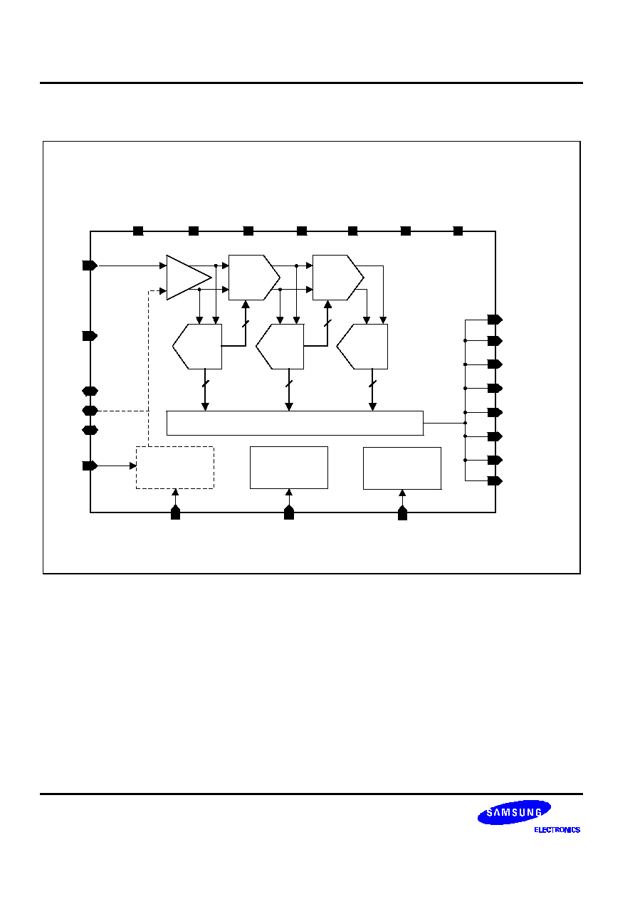
FUNCTIONAL BLOCK DIAGRAM
Reference
Generator
AI8
RP8
DO8[4]
DO8[7](MSB)
DO8[6]
DO8[5]
RM8
RS8
SAH
Digital Corection Logic
4-bit
Flash
DO8[3]
DO8[2]
DO8[1]
CK8
AVDD25D
AVBB25A
AVSS25A
AVDD25A
AVSS25D
AVBB25D
AVDD12D
DO8[0] (LSB)
PD8
REF8
MDAC1
MDAC2
RN8
SU8
Bias Current
Generator
Clock
Generator
3-bit
Flash
3-bit
Flash
4 bits
3 bits
3 bits
Ver 1.3 (Jun. 2002)
This data sheet is a preliminary version. No responsibility is assumed by SEC for its use nor for any infringements of patents
or other rights of third parties that may result from its use. The content of this data sheet is subject to change without any
notice.
ADC1394X
0.13
µ
µ
m 8-BIT 20MSPS ADC
3
CORE PIN DESCRIPTION
Name
I/O Type
I/O Pad
Pin Description
AI8
AI
pmiar50_abb
Positive analog input
CK8
DI
pmicc_abb
Clock input (20MHz)
PD8
DI
pmicc_abb
Power down (active high)
REF8
AB
pmoar50_abb
External 1.2V source
RN8
AB
pmoa_abb
Negative reference voltage (0.45V)
RP8
AB
pmoa_abb
Positive reference voltage (1.35V)
RM8
AB
pmoa_abb
Mid reference voltage (internally generated)
RS8
DI
pmicc_abb
Internal/external reference selection
High: Internal reference
Low: External reference
SU8
DI
pmicc_abb
ADC speed up
DO8[7:0]
DO
pmob8_abb
Digital output
AVDD25A8
AP
vdd25tm_abb
Analog power (+2.5V)
AVSS25A8
AG
vsstm_abb
Analog ground (0.0V)
AVBB25A8
AG
vbbm_abb
Analog substrate bias (0.0V)
AVDD25D8
DP
vdd25tm_abb
Digital power (+2.5V)
AVSS25D8
DG
vsstm_abb
Digital ground (0.0V)
AVBB25D8
DG
vbbm_abb
Digital substrate bias (0.0V)
AVDD12D8
DP
vdd12im_abb
Digital power for internal level shifter
I/O
Type
Abbr.
-- AI: Analog Input
-- DI: Digital Input
-- AO: Analog Output
-- DO: Analog Output
-- AP: Analog Power
-- AG: Analog Ground
-- DP: Digital Power
-- DG: Digital Ground
-- AB: Analog Bi-Direction
-- DB: Digital Bi-Direction
0.13
µ
µ
m 8-BIT 20MSPS ADC
ADC1394X
4
CORE CONFIGURATION
AI8
DO8[4]
DO8[7](MSB)
DO8[6]
DO8[5]
AVSS25A8
AVBB25A8
RS8
RP8
AVDD25D8
AVDD25A8
AVSS25D8
AVBB25D8
adc1394x
RN8
REF8
AVDD12D8
DO8[0] (LSB)
DO8[3]
DO8[2]
DO8[1]
PD8
SU8
CK8
RM8
Voltage Reference
Generator
A Channel
ADC1394X
0.13
µ
µ
m 8-BIT 20MSPS ADC
5
ABSOLUTE MAXIMUM RATINGS
Characteristic
Symbol
Value
Unit
Supply voltage
AVDD25A8
AVDD25D8
3.6
V
AVDD12D8
1.5
Analog input voltage
AI8
AVSS25A8 to AVDD25A8
V
Digital input voltage
CK8
AVSS25D8 to AVDD25D8
V
Digital output voltage
V
OH
, V
OL
AVSS25D8 to AVDD25D8
V
Storage temperature range
Tstg
≠45 to 150
∞
C
NOTES:
1.
Absolute maximum rating specifies the values beyond which the device may be damaged permanently. Exposure
to absolute maximum rating conditions for extended periods may affect reliability. Each condition value is applied
with the other values kept within the following operating conditions and function operation under any of these conditions
is
not implied.
2.
All
voltages
are
measured
with
respect
to
AVSS25A8/AVSS25D8
unless
otherwise
specified.
3.
100pF
capacitor
is
discharged
through
a
1.5k
resistor
(Human
body
model)
RECOMMENDED OPERATING
CONDITIONS
Characteristics
Symbol
Min
Typ
Max
Unit
Supply voltage
AVDD25A8
AVDD25D8
2.3
2.5
2.7
V
AVDD12D8
1.1
1.2
1.3
Reference input voltage (externally)
RP8
RN8
≠
≠
1.35
0.45
≠
≠
V
Analog input voltage (+)
AI8
0.0
≠
1.8
V
Analog input voltage (-)
RM8
≠
0.9
≠
V
Operating temperature
Topr
≠10
≠
70
∞
C
NOTES:
1.
It
is
strongly
recommended
that
all
the
supply
pins
(AVDD25A8,
AVDD25D8)
be
powered
from
the
same
source
to
avoid
power
latch-up.
2.
Reference Input Voltage REF8, RP8 and RN8 are generated internally and can be forced externally.
3.
In case that AVDD12D8 be connected to 1.2V power line of Digital Part during Full Chip Layout of Mixed Chip, a care
should be taken into the Test Vector Generation to insure at least one of the 1.2V Power Source of Digital Part, which
would be finally connected to ADC1394X through any indirect path, to be alive during the ADC Test Mode, because, in
general, 1.2V digital power could be down with Digital Part for Analog Core Test of Analog/Digital Mixed Chip.
0.13
µ
µ
m 8-BIT 20MSPS ADC
ADC1394X
6
DC ELECTRICAL
CHARACTERISTICS
Characteristics
Symbol
Min
Typ
Max
Unit
Conditions
Resolution
≠
≠
≠
8
Bits
≠
Differential linearity error
DLE
≠
≠
±
1.0
LSB
≠
Integral linearity error
ILE
≠
≠
±
1.0
LSB
≠
Bottom offset voltage error
EOB
≠
≠
10
LSB
≠
Top offset voltage error
EOT
≠
≠
10
LSB
≠
NOTE: Converter
specifications
(unless
otherwise
specified)
AVDD25A8=2.5V
AVDD25D8=2.5V
AVDD12D8=1.2V
AVSS25A8=GND
AVSS25D8=GND
AVBB25A8=GND
AVBB25D8=GND
RP8=1.35V
RN8=0.45V
PD8=Low
SU8=Low
RS8=Low
Ta=25
∞
C
AC ELECTRICAL CHARACTERISTICS
Characteristics
Symbol
Min
Typ
Max
Unit
Conditions
Maximum conversion rate
fc
≠
≠
20
MSPS
≠
Dynamic supply current
Ivdd
≠
18
mA
fc = 20MHz
(without system load)
Power down current
Ipd
≠
≠
0.8
mA
Ipd=I(AVDD25A8)+I(AVDD25D8)
Power-on settling time
Tset
0.3
≠
≠
us
See
"Delay Timing Diagram"
Digital output data delay
Td
≠
4
≠
ns
See
"Timing Diagram"
Signal - to - noise ratio
SNR
38
42
≠
dB
AI8 = 1MHz
fc = 20MHz
ADC1394X
0.13
µ
µ
m 8-BIT 20MSPS ADC
7
INPUT-OUTPUT MAPPING TABLE
Index
AI8 Input (V)
RM8 (V)
Digital Output
0
0.00000 ~ 0.00703
0.9
(Internally generated)
00000000
1LSB = 7.03125mV for
single input
1
0.00703 ~ 0.01406
00000001
RP8 = 1.35V
2
0.01406 ~ 0.02109
00000010
RN8 = 0.45V
∑
∑
∑
∑
∑
∑
∑
∑
∑
127
0.89297 ~ 0.90000
01111111
128
0.90000 ~ 0.90703
10000000
129
0.90703 ~ 0.91406
10000001
∑
∑
∑
∑
∑
∑
∑
∑
∑
253
1.77891 ~ 1.78594
11111101
254
1.78594 ~ 1.79297
11111110
255
1.79297 ~ 1.80000
11111111
0.13
µ
µ
m 8-BIT 20MSPS ADC
ADC1394X
8
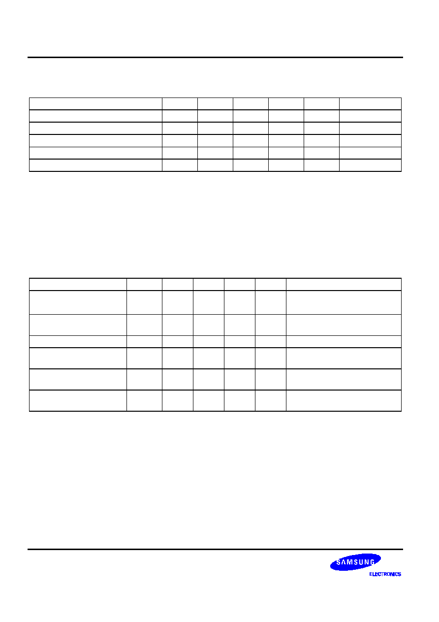
TIMING DIAGRAM
AI
CK
DO
AI(4)
AI(5)
AI(6)
AI(7)
Td
AI(3)
STC
AI(8)
2.5 Clock Pipeline Delay
DO[0]
DO[1]
DO[2]
DO[3]
DO[4]
ADC1394X
0.13
µ
µ
m 8-BIT 20MSPS ADC
9
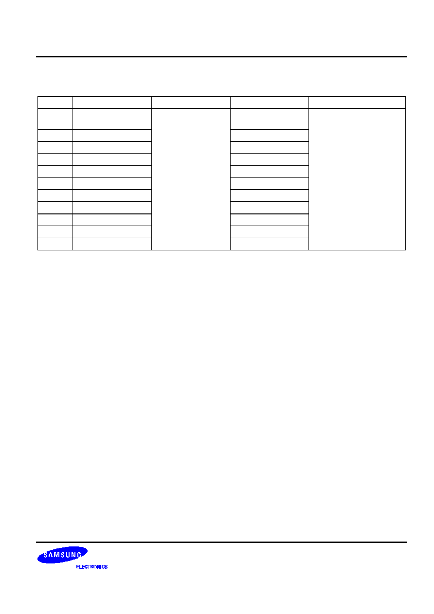
DELAY TIMING DIAGRAM
CK8
DO8
PD8
RS8
RSS8
Cannot be Changed
Can be Changed
50us
Set-Up Time
. . .
. . .
. . .
. . .
(Stabilization Delay
0.3us Power-On Settling Time
DO8(0)
DO8(0)
DO8(a)
INVALID
INVALID
T
d
NOTES:
1.
Reference Control Input(RS8) should not be changed during ADC operation (while PD8 is LOW)
2.
During ADC power down (while PD8 is HIGH), external source must be kept forced.
3.
Reference Control Inputs can be set during PD8 LOW, with set-up timing constraint of at least 50us.
4.
Although certain digital outputs would be presented on the DO8 right after PD8 goes LOW, those should be disregarded
for at 0.3us Stabilization Delay. That's because it takes time for the internal nodes of ADC to be stabilized after Power-
On
to operate correctly and produce the valid Digital Outputs.
0.13
µ
µ
m 8-BIT 20MSPS ADC
ADC1394X
10
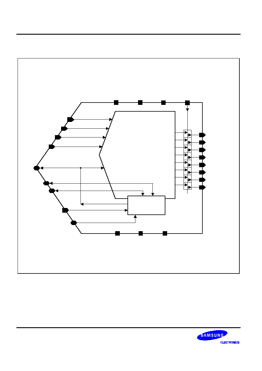
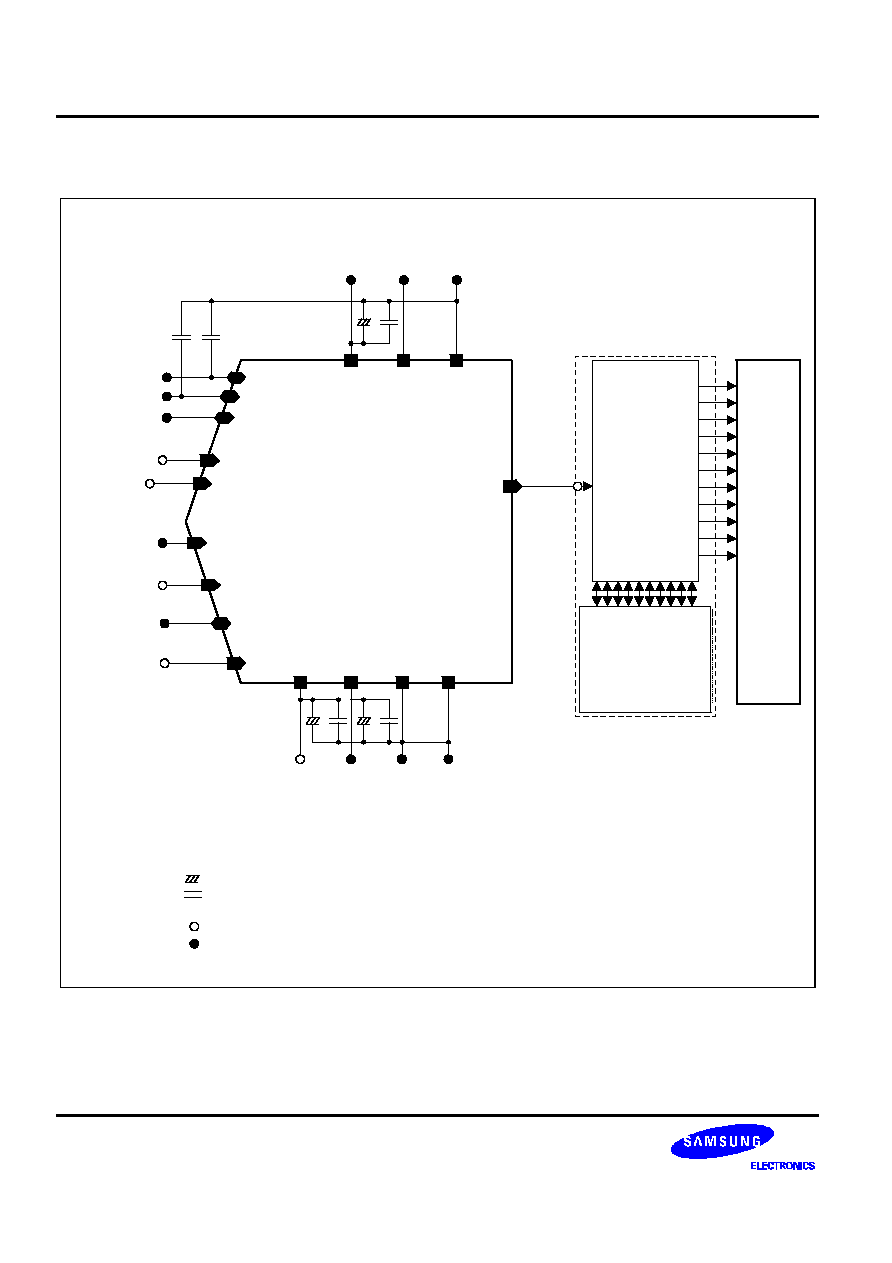
CORE EVALUATION GUIDE
MUX
Host
DSP
Core
CK8
DO8[7:0]
RP8
adc1394x
AVDD25A8
RS8
AVDD25D8
AVSS25D8
AVBB25D8
AVDD12D8
RN8
REF8
AI8
RM8
SU8
PD8
AVSS25A8
AVBB25A8
+2.5V Analog
Power for
ADC
Analog GND
for ADC
Bi-Directional PAD
ADC Function
Measuring & Digital
Input Forcing
1.35V
0.45V
Low
Low
0.0V ~ +1.8V
20MHz
1.2V
Low
Digital GND
for ADC
+2.5V Digital
Power for
Level Shifter
+2.5V Digital
Power for
ADC
NOTES:
: 10uF electronic capacitor unless otherwise specified
: 0.1uF ceramic capacitor unless otherwise specified
: Dedicated Pins
: Sharable Pins
ADC1394X
0.13
µ
µ
m 8-BIT 20MSPS ADC
11
USER GUIDE
1. Input Signal Range
The adc1394x is designed to use single mode input.
< Single Mode Input Condition >
Pins
Input Range
Conditions
AI8
0.0V ~ 1.8V
RM8
0.9V
Internally generated by the function of (RP8+RN8)/2
2. Input Signal Speed
Normal speed range of adc1394x is 1MHz ~ 6MHz input quantized by 20MHz clock, which is fixed by a normal
video signal format. To use the input of adc1394x on near nyquist ranges such as the direct IF processing,
consult about the additional performance issues with SEC.
0.13
µ
µ
m 8-BIT 20MSPS ADC
ADC1394X
12
FEEDBACK
REQUEST
It should
be
quite
helpful
to
our
ADC
core
development
if
you
specify
your
system
requirements
on
ADC
in
the
following
characteristic
checking
table
and
fill
out
the
additional
questions.
We
appreciate
your
interest
in
our
products.
Thank
you
very
much.
Characteristic
Min
Typ
Max
Unit
Remarks
Analog power supply voltage
V
Digital power supply voltage
V
Bit resolution
Bit
Reference input voltage
V
Analog input voltage
Vpp
Operating temperature
∞
C
Integral non-linearity error
LSB
Differential non-linearity error
LSB
Bottom offset voltage error
mV
Top offset voltage error
mV
Maximum conversion rate
MSPS
Dynamic supply current
mA
Power dissipation
mW
Signal-to-noise ratio + distortion ratio
dB
Pipeline delay
CLK
Digital output format (provide detailed
description & timing diagram)
-- Between single input-output and differential input-output configurations, which one is suitable for your system
and why?
-- Please comment on the internal/external pin configurations you want our ADC to have, if you have any
reason to prefer some type of configuration.
-- Freely list those functions you want to be implemented in our ADC, if you have any.
ADC1394X
0.13
µ
µ
m 8-BIT 20MSPS ADC
13
HISTORY CARD
Version
Date
Modified Items
Comments
Ver1.0
02. 04.18
Original version published (preliminary)
Ver1.1
02. 06. 04
Modify REF8 I/O pad type in core pin description on page 2.
Ver1.2
02. 06. 19
Plus 0.1uF cap with RM8 pin at core evaluation guide on page 9.
Ver1.3
02. 06. 20
Cancell the issue of ver.1.2